AD7226(RevA) Ver la hoja de datos (PDF) - Analog Devices
Número de pieza
componentes Descripción
Fabricante
AD7226 Datasheet PDF : 12 Pages
| |||
AD7226
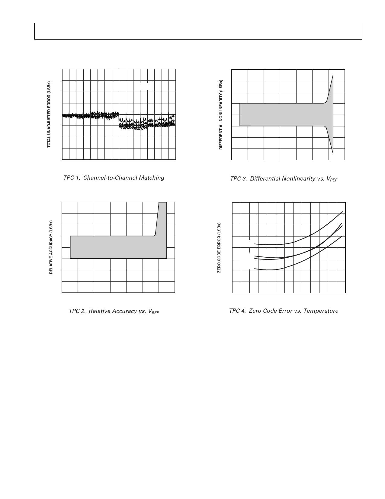
Figure 9. Zero Code Error vs. Temperature
Figure 10. Dynamic Response (VSS = –5 V)
SPECIFICATION RANGES
In order for the DACs to operate to their specifications, the ref-
erence voltage must be at least 4 V below the VDD power supply
voltage. This voltage differential is required for correct genera-
tion of bias voltages for the DAC switches.
The AD7226 is specified to operate over a VDD range from
+12 V ± 5% to +15 V ± 10% (i.e., from +11.4 V to +16.5 V)
with a VSS of –5 V ± 10%. Operation is also specified for a
single +15 V ± 5% VDD supply. Applying a VSS of –5 V results
in improved zero code error, improved output sink capability
with outputs near AGND and improved negative-going settling-
time.
Performance is specified over a wide range of reference voltages
from 2 V to (VDD – 4 V) with dual supplies. This allows a range
of standard reference generators to be used such as the AD580,
a +2.5 V bandgap reference and the AD584, a precision +10 V
reference. Note that in order to achieve an output voltage range
of 0 V to +10 V a nominal +15 V ± 5% power supply voltage is
required by the AD7226.
SETTLING TIME
The output stage of the buffer amplifiers consists of a bipolar
NPN transistor from the VDD line and a constant current load to
VSS. VSS is the negative power supply for the output buffer am-
plifiers. As mentioned in the op amp section, in single supply
operation the NMOS transistor will come out of saturation as
the output voltage approaches AGND and will act as a resistive
load of approximately 2 kΩ to AGND. As a result, the settling-
time for negative-going signals approaching AGND in single
supply operation will be longer than for dual supply operation
where the current load of 400 µA is maintained all the way down
to AGND. Positive-going settling-time is not affected by VSS.
The settling-time for the AD7226 is limited by the slew-rate of
the output buffer amplifiers. This can be seen from Figure 10
which shows the dynamic response for the AD7226 for a full
scale change. Figures 11a and 11b show expanded settling-time
photographs with the output waveforms derived from a differen-
tial input to an oscilloscope. Figure 11a shows the settling-time
for a positive-going step and Figure 11b shows the settling-time
for a negative-going output step.
Figure 11a. Positive-Step Settling-Time (VSS = –5 V)
Figure 11b. Negative-Step Settling-Time (VSS = –5 V)
GROUND MANAGEMENT
AC or transient voltages between AGND and DGND can cause
noise at the analog output. This is especially true in micropro-
cessor systems where digital noise is prevalent. The simplest
method of ensuring that voltages at AGND and DGND are
equal is to tie AGND and DGND together at the AD7226. In
more complex systems where the AGND and DGND intertie is
on the backplane, it is recommended that two diodes be con-
nected in inverse parallel between the AD7226 AGND and
DGND pins (IN914 or equivalent).
REV. A
–7–
Share Link: 