IDT723614L30PQF Ver la hoja de datos (PDF) - Integrated Device Technology
Número de pieza
componentes Descripción
Fabricante
IDT723614L30PQF
Integrated Device Technology

IDT723614L30PQF Datasheet PDF : 39 Pages
| |||
IDT723614 CMOS SyncBiFIFO™ WITH BUS MATCHING AND BYTE SWAPPING
64 x 36 x 2
COMMERCIAL TEMPERATURE RANGE
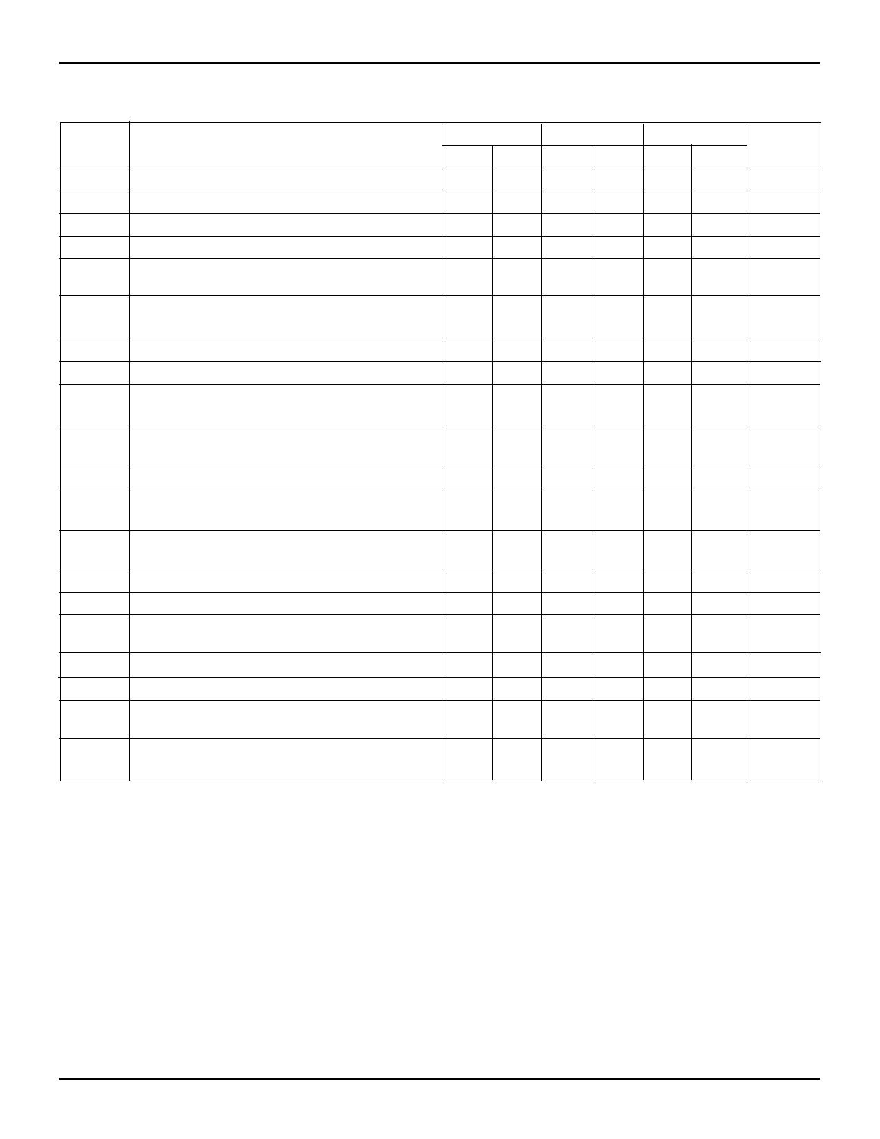
DC ELECTRICAL CHARACTERISTICS OVER RECOMMENDED RANGES OF SUPPLY VOLTAGE
AND OPERATING FREE-AIR TEMPERATURE (See Figures 4 through 26)
IDT723614L15 IDT723614L20 IDT723614L30
Symbol
Parameter
Min. Max. Min. Max. Min. Max.
fS
Clock Frequency, CLKA or CLKB
– 66.7 –
50
– 33.4
tCLK
Clock Cycle Time, CLKA or CLKB
15
–
20
–
30
–
tCLKH Pulse Duration, CLKA and CLKB HIGH
6
–
8
–
12
–
tCLKL Pulse Duration, CLKA and CLKB LOW
6
–
8
–
12
–
tDS
Setup Time, A0-A35 before CLKA↑ and B0-B35 4
–
5
–
6
–
before CLKB↑
tENS
Setup Time, CSA, W/RA, ENA and MBA before 5
–
5
–
6
–
CLKA↑; CSB,W/RB and ENB before CLKB↑
tSZS
Setup Time, SIZ0, SIZ1,and BE before CLKB↑
4
–
5
–
6
–
tSWS
Setup Time, SW0 and SW1 before CLKB↑
5
–
7
–
8
–
tPGS
Setup Time, ODD/EVEN and PGA before
4
–
5
–
6
–
CLKA↑; ODD/EVEN and PGB before CLKB↑(1)
tRSTS
Setup Time, RST LOW before CLKA↑
or CLKB↑(2)
5
–
6
–
7
–
tFSS
Setup Time, FS0 and FS1 before RST HIGH
5
–
6
–
7
–
tDH
Hold Time, A0-A35 after CLKA↑ and B0-B35
after CLKB↑
tENH
Hold Time, CSA, W/RA, ENA and MBA after
CLKA↑; CSB, W/RB, and ENB after CLKB↑
tSZH
Hold Time, SIZ0, SIZ1, and BE after CLKB↑
1
–
1
–
1
–
1
–
1
–
1
–
2
–
2
–
2
–
tSWH
Hold Time, SW0 and SW1 after CLKB↑
0
–
0
–
0
–
tPGH
Hold Time, ODD/EVEN and PGA after CLKA↑;
0
–
0
–
0
–
ODD/EVEN and PGB after CLKB↑(1)
tRSTH Hold Time, RST LOW after CLKA↑ or CLKB↑(2)
5
–
6
–
7
–
tFSH
Hold Time, FS0 and FS1 after RST HIGH
4
–
4
–
4
–
tSKEW1(3) Skew Time, between CLKA↑ and CLKB↑
for EFA, EFB, FFA, and FFB
8
–
8
–
10
–
tSKEW2(3) Skew Time, between CLKA↑ and CLKB↑
for AEA, AEB, AFA, and AFB
9
–
16
–
20
–
Unit
MHz
ns
ns
ns
ns
ns
ns
ns
ns
ns
ns
ns
ns
ns
ns
ns
ns
ns
ns
ns
NOTES:
1. Only applies for a clock edge that does a FIFO read.
2. Requirement to count the clock edge as one of at least four needed to reset a FIFO.
3. Skew time is not a timimg constraint for proper device operation and is only included to illustrate the timing relationship between CLKA cycle and
CLKB cycle.
10
Share Link: