TPC8125 Ver la hoja de datos (PDF) - Toshiba
Número de pieza
componentes Descripción
Fabricante
TPC8125 Datasheet PDF : 7 Pages
| |||
TPC8125
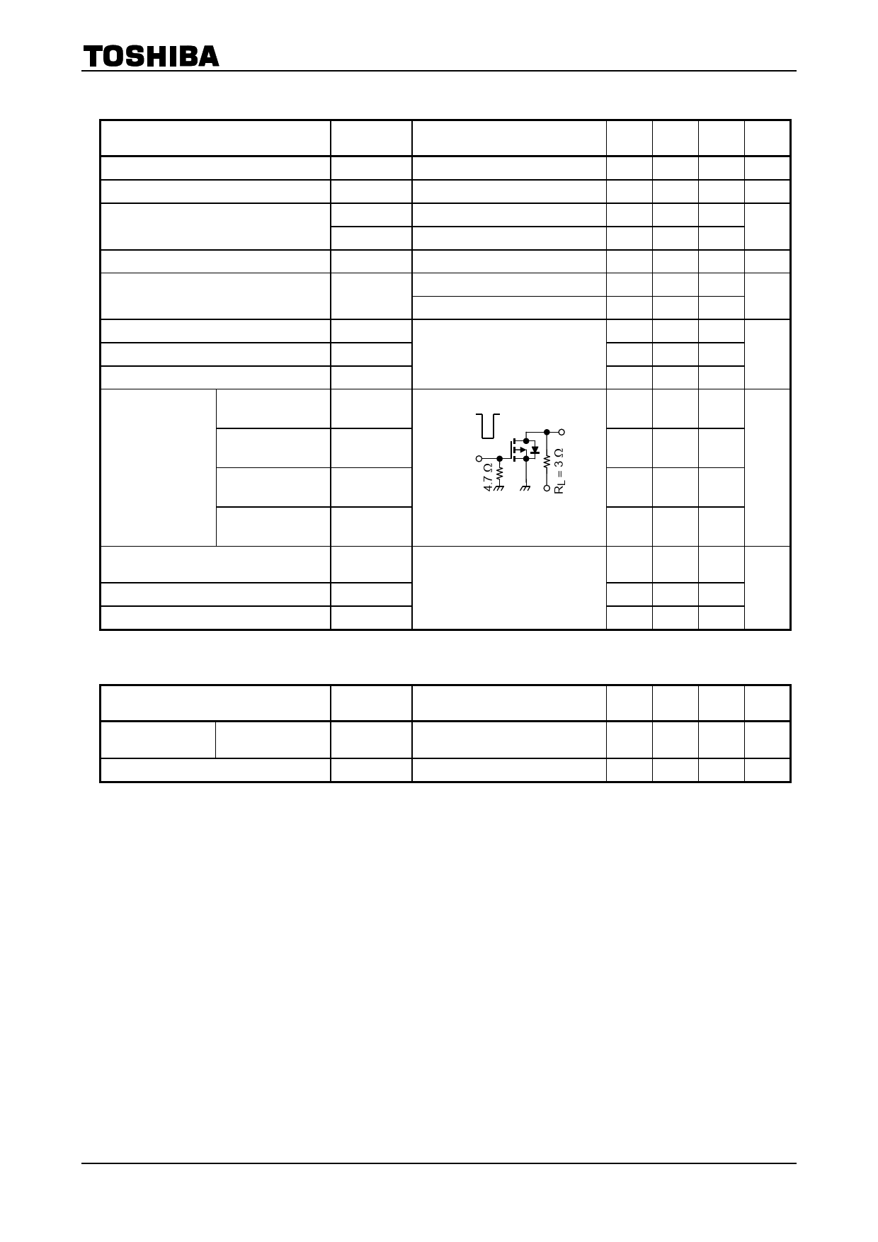
Electrical Characteristics (Ta = 25°C)
Characteristics
Gate leakage current
Drain cut-OFF current
Drain-source breakdown voltage
Gate threshold voltage
Drain-source ON-resistance
Input capacitance
Reverse transfer capacitance
Output capacitance
Rise time
Switching time
Turn-ON time
Fall time
Turn-OFF time
Total gate charge
(gate-source plus gate-drain)
Gate-source charge 1
Gate-drain (“miller”) charge
Symbol
Test Condition
Min Typ. Max Unit
IGSS
VGS = ±20 V, VDS = 0 V
⎯
⎯ ±100 nA
IDSS
VDS = −30 V, VGS = 0 V
⎯
⎯
−10
μA
V (BR) DSS ID = −10 mA, VGS = 0 V
−30 ⎯
⎯
V
V (BR) DSX ID = −10 mA, VGS = 10 V (Note 6) −21
⎯
⎯
Vth
VDS = −10 V, ID = −0.5 mA
−0.8 ⎯
−2.0
V
RDS (ON)
VGS = −4.5 V, ID = −5 A
VGS = −10 V, ID = −5 A
⎯
13
17
mΩ
⎯
10
13
Ciss
⎯ 2580 ⎯
Crss
VDS = −10 V, VGS = 0 V, f = 1 MHz ⎯
430
⎯
pF
Coss
⎯
490
⎯
tr
0V
VGS
−10 V
ton
tf
ID = −5 A
⎯
8
⎯
VOU
⎯
16
⎯
ns
⎯
75
⎯
VDD ≈ −15 V
toff
Duty ≤ 1%, tw = 10 μs
⎯
245
⎯
Qg
Qgs1
Qgd
VDD ≈ −24 V, VGS = −10 V,
ID = −10 A
⎯
64
⎯
⎯
6
⎯
nC
⎯
17
⎯
Source-Drain Ratings and Characteristics (Ta = 25°C)
Characteristics
Drain reverse
current
Pulse
Forward voltage (diode)
(Note 1)
Symbol
Test Condition
IDRP
VDSF
⎯
IDR = −10 A, VGS = 0 V
Min Typ. Max Unit
⎯
⎯
−40
A
⎯
⎯
1.2
V
Note 6: VDSX mode (the application of a plus voltage between gate and source) may cause decrease in maximum
rating of drain-source voltage.
3
2009-11-17
Share Link: 