TOP222G-TL Ver la hoja de datos (PDF) - Power Integrations, Inc
Número de pieza
componentes Descripción
Fabricante
TOP222G-TL Datasheet PDF : 20 Pages
| |||
TOP221-227
TOPSwitch-II Family Functional Description
TOPSwitch is a self biased and protected linear control current-
to-duty cycle converter with an open drain output. High
efficiency is achieved through the use of CMOS and integration
of the maximum number of functions possible. CMOS process
significantly reduces bias currents as compared to bipolar or
discrete solutions. Integration eliminates external power
resistors used for current sensing and/or supplying initial start-
up bias current.
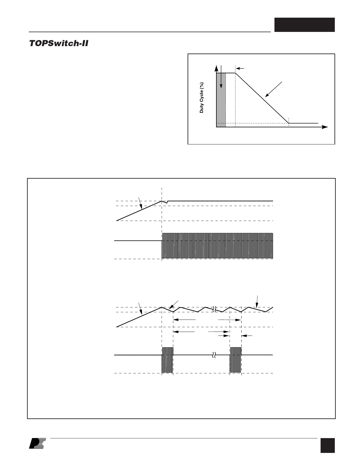
Auto-restart
IB
DMAX
Slope = PWM Gain
During normal operation, the duty cycle of the internal output
MOSFET decreases linearly with increasing CONTROL pin
current as shown in Figure 4. To implement all the required
control, bias, and protection functions, the DRAIN and
CONTROL pins each perform several functions as described
below. Refer to Figure 2 for a block diagram and to Figure 6 for
timing and voltage waveforms of the TOPSwitch integrated
circuit.
DMIN
ICD1 2.0
6.0
IC (mA)
PI-2040-050197
Figure 4. Relationship of Duty Cycle to CONTROL Pin Current.
5.7 V
4.7 V
VC
0
IC
Charging CT
DRAIN VIN
Off
0
5.7 V
VC 4.7 V
0
IC
Charging CT
Switching
(a)
ICD1
Discharging CT
ICD2
Discharging CT
8 Cycles
95%
5%
DRAIN VIN
0
Off
Off
Off
Switching
(b)
Switching
CT is the total external capacitance
connected to the CONTROL pin
Figure 5. Start-up Waveforms for (a) Normal Operation and (b) Auto-restart.
PI-1956-092496
3 D
7/01
Share Link: 