TN2425TG Ver la hoja de datos (PDF) - Supertex Inc
Número de pieza
componentes Descripción
Fabricante
TN2425TG Datasheet PDF : 5 Pages
| |||
TN2425TG
Electrical Characteristics (each device, TJ=25°C unless otherwise specified)
Symbol Parameter
Min
Typ
Max
Units
Conditions
BVDSS Drain-to-source breakdown voltage
250
-
-
V
VGS = 0V, ID = 250µA
VGS(th)
ΔVMatch
ΔVGS(th)
Gate threshold voltage
Change in VGS(th) with temperature
VGS(th) change with temperature
0.6
-
2.0
V
VGS = VDS, ID = 1mA
-
-
25
mV
VGS = VDS, ID = 1mA,
TA = 10OC - 80OC
-
-
-5.0 mV/OC VGS = VDS, ID = 1mA
IGSS
Gate body leakage current
-
-
100
nA VGS = ±20V, VDS = 0V
IDSS
Zero gate voltage drain current
-
-
10
µA VDS = Max rating, VGS = 0V
-
-
1.0
mA
V = 0.8 Max Rating,
DS
VGS = 0V, TA = 125OC
ID(ON) ON-state drain current
1.5
-
-
1.8
-
-
A
VGS = 6.0V, VDS = 25V
VGS = 10V, VDS = 25V
RDS(ON)
Static drain-to-source ON-state
resistance
-
-
5.0
Ω
VGS = 4.5V, ID = 300mA
-
-
3.5
VGS = 10V, ID = 400mA
RMATCH Channel to channel RDS(ON) matching
-
-
20
%
VGS = 10V, ID = 400mA
ΔRDS(ON) Change in RDS(ON) with temperature
-
-
1.4
%/OC VGS = 10V, ID = 400mA
GFS
Forward transconductance
300
-
-
mmho VDS = 15V, ID = 400mA
GFSMATCH Channel to channel GFS matching
-
-
5
%
VDS = 15V, ID = 50mA
-
-
5
%
VGS = 15V, ID = 1.50A
CISS
Input capacitance
-
115 200
COSS Common source output capacitance
-
30 100
pF VGS = 0V, VDS = 25V, f = 1MHz
CRSS Reverse transfer capacitance
-
10
40
CISSMATCH Channel to channel CISS matching
-
-
25
COSSMATCH Channel to channel COSS matching
-
-
25
%
VGS = 0V, VDS = 25V, f = 1MHz
CRSSMATCH Channel to channel CRSS matching
-
-
25
td(ON)
Turn-ON delay time
-
5
15
tr
td(OFF)
Rise time
Turn-OFF delay time
-
10
25
-
25
35
ns
VDD = 25V, ID = 500mA,
RGEN = 25Ω
tf
Fall time
-
5
15
VSD
Diode forward voltage drop
-
-
1.8
V
VGS = 0V, ISD = 500mA
trr
Reverse recovery time
-
300
-
ns VGS = 0V, ISD = 500mA
Notes:
1.All D.C. parameters 100% tested at 25OC unless otherwise stated. (Pulse test: 300µs pulse, 2% duty cycle.)
2.All A.C. parameters sample tested.
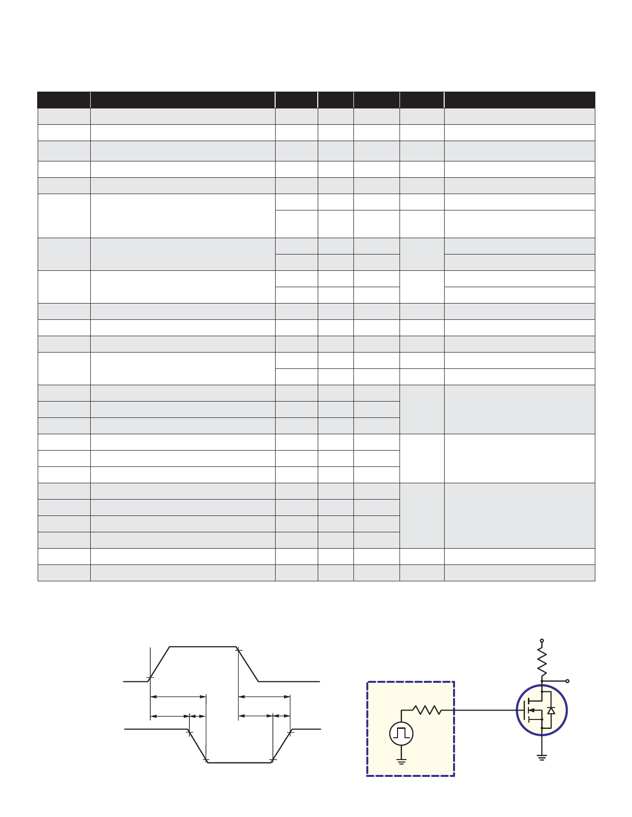
Switching Waveforms and Test Circuit
10V
INPUT
90%
0V 10%
t(ON)
t(OFF)
td(ON)
tr
td(OFF)
tF
VDD
OUTPUT
0V
10%
90%
10%
90%
PULSE
GENERATOR
RGEN
INPUT
VDD
RL
OUTP
D.U.T.
2
Share Link: 