TLP554 Ver la hoja de datos (PDF) - Toshiba
Número de pieza
componentes Descripción
Fabricante
TLP554 Datasheet PDF : 8 Pages
| |||
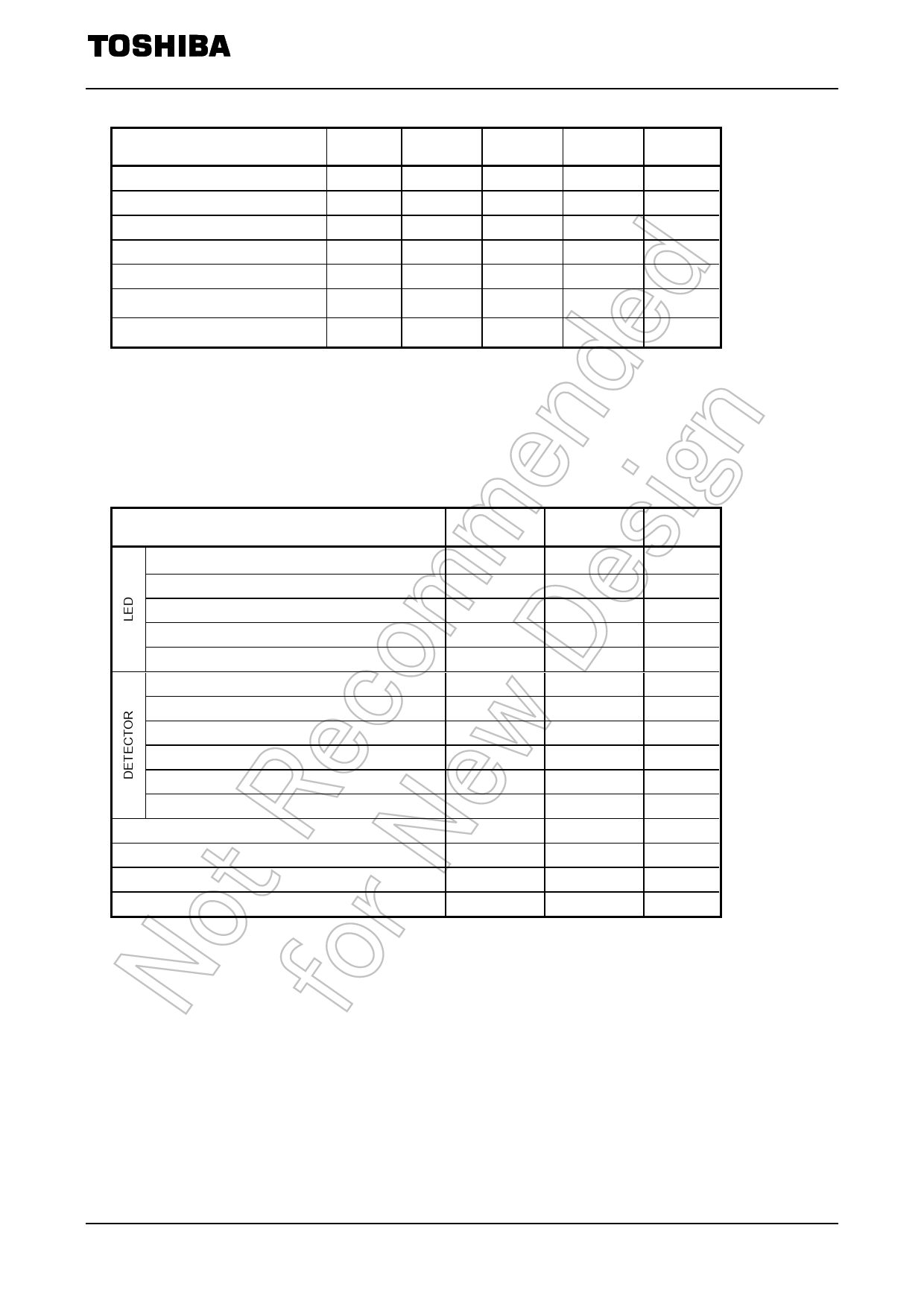
Recommended Operating Conditions
TLP554
Characteristic
Symbol
Min
Typ.
Max
Unit
Low Level input Voltage
VFL
-3
0
High Level input current
IFH
6.3 (Note 1)
―
Supply Voltage
(Note 2)
VCC
4.5
5
High-Level Enable Voltage
VEH
2.0
―
Low-Level Enable Voltage
VEL
0
―
Fan Out(TTL Load)
N
―
―
Operating Temperature
Topr
0
―
1.0
V
20
mA
5.5
V
VCC
V
0.8
V
8
―
70
°C
Note: Recommended operating conditions are given as a design guideline to obtain expected performance of the
device. Additionally, each item is an independent guideline respectively. In developing designs using this
product, please confirm specified characteristics shown in this document.
Note 1: 6.3 mA condition permits at least 20 % CTR degradation. Initial switching threshold is 5.0 mA or less.
Note 2: Denotes the operating range, not the recommended operating condition.
Absolute Maximum Ratings (Ta = 25°C)
Characteristic
Symbol
Rating
Unit
Forward current
Forward current derating
Reverse voltage
Input power dissipation
Input power dissipation derating
Output current
Output voltage
Supply voltage
Enable voltage
Output power dissipation
Output power dissipation derating
Storage temperature range
Operating temperature range
Lead soldering temperature (10 s)
Isolation voltage (AC, 60 s, R.H.≤ 60 %)
(Ta > 85°C)
(Ta > 85°C)
(Note 1)
(Note 2)
(Ta > 85°C)
(Note 3)
(Note 4)
IF
ΔIF/ΔTa
VR
PD
ΔPD/°C
IO
VO
VCC
VE
PO
ΔPo/ΔTa
Tstg
Topr
Tsol
BVS
20
-1.6
5
100
-2.5
25
-0.5 to 7
7
5.5
40
-2.6
-55 to 125
-40 to 85
260
2500
mA
mA/°C
V
mW
mW/°C
mA
V
V
V
mW
mW/°C
°C
°C
°C
Vrms
Note: Using continuously under heavy loads (e.g. the application of high temperature/current/voltage and the
significant change in temperature, etc.) may cause this product to decrease in the reliability significantly even
if the operating conditions (i.e. operating temperature/current/voltage, etc.) are within the absolute maximum
ratings and the operating ranges.
Please design the appropriate reliability upon reviewing the Toshiba Semiconductor Reliability Handbook
(“Handling Precautions”/“Derating Concept and Methods”) and individual reliability data (i.e. reliability test
report and estimated failure rate, etc).
Note 1: 60 s Maximum.
Note 2: Not to exceed VCC by more than 500 mV.
Note 3: 2 mm below seating plane.
Note 4: Device considered a two-terminal device :Pins 1, 2, 3 and 4 shorted together,and Pins 5, 6, 7 and 8 shorted
together.
© 2019
2
Toshiba Electronic Devices & Storage Corporation
2019-06-24
Share Link: 