TEA2029C Ver la hoja de datos (PDF) - STMicroelectronics
Número de pieza
componentes Descripción
Fabricante
TEA2029C Datasheet PDF : 9 Pages
| |||
TEA2029C
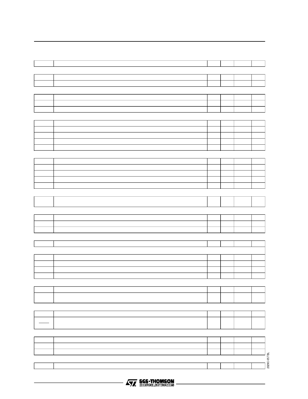
ELECTRICAL OPERATING CHARACTERISTICS (continued)
Symbol
Parameter
Min. Typ. Max. Unit
PHASE COMPARATOR ϕ2 (Pin 16)
I16 Charging Current
Delay between the Edges of ϕ1 and ϕ2 (fVCO = 500kHz)
0.4 0.6 0.8 mA
1.5 2
2.8 µs
LINE OUTPUT (OPEN COLLECTOR) (Pin 10)
Output Voltage (I10max = 20mA)
1
1.5
V
T10 Output Pulse Duration (when fly-back pulse is with in time T10) (fVCO = 500kHz) 24 26
30
µs
∆t ϕ2 Phase Range
15 16 19 µs
FRAME LOGIC
Free Running Period (with mute signal)
315
Line
Search Window
50Hz Window
60Hz Window
247
361 Line
309
315 Line
247
276 Line
VCR Mode Window
247
361 Line
FRAME SAW-TOOTH GENERATOR (Pins 3-5)
I5(60)
VS
Saw-tooth Amplitude
SInternal Current Generator (60Hz on)
Discharging Time (with C = 0.47µF, ∆V < 4V)
Starting Level (0mA < IS < 0mA)
Saw-tooth Amplitude (IS = 10mA)
23
4
VPP
12 14 16 µA
50
70 µs
1 1.26 1.4 V
23
4
VPP
FRAME FEEDBACK INPUTS (Pins 1-2)
I1,2 Positive and Negative Input Current (V1 - V2) > 25mA for frame blanking
safety
10 µA
FRAME OUPUT (Pin 4)
Output Voltage (0mA < |I4| < 80mA)
TON max (fVCO = 500kHz)
Output Phase Range
10
V
36 40 41 µs
0
tON max
SMPS CONTROL INPUT (Pin 9)
I9
Input Current (V9 = Vref 14)
2
µA
SMPS OUTPUT (Pin 7) - No Relation between End of SMPS Pulse (pin 7) and Leading Edge of Line Flyback (pin 12)
V7 Output Voltage (0 < I7 < 20mA)
T7
tON max (fVCO = 500kHz)
Nominal Time (V9 = Vref 14)
Output Phase Range
10
V
30 32 34 µs
26
31 µs
0
tON max µs
SAFETY INPUT (Pin 28)
V28 Threshold Voltage (V28 = Vref 14)
Input Current (if V28 > Vref 14 then SMPS, line and frame are switched off
during the next line retrace)
1.15 1.26 1.37 V
3
µA
SWITCH-ON, SWITCH-OFF PROCESSING (Pin 15)
Ich 15
Ich 15
Idis 15
Charging Current (tC = 4µs, T = 64µs)
Ratio Charging/discharging
70
0.8 1
130 µA
1.2 µA
STARTING SUPPLY VOLTAGE (Pin 8)
VCC SMPS*, Frame and Line Starting (pins 7, 10 and 4)
VCC SMPS Stopping during Line Retrace
VCC Frame and Line Stopping
5.25
6.5 V
5.25
6.5 V
5.25
6.5 V
CURRENT REFERENCE (PIn 14)
Vref 14 Voltage Reference
1.2 1.26 1.35 V
6/9
Share Link: 