TEA6323 Ver la hoja de datos (PDF) - Philips Electronics
Número de pieza
componentes Descripción
Fabricante
TEA6323 Datasheet PDF : 36 Pages
| |||
Philips Semiconductors
Sound fader control circuit
Preliminary specification
TEA6323T
The last section of the circuit is the volume II block. The
balance and fader functions are performed using the same
control blocks. This is realized by 4 independently
controllable attenuators, one for each output. The control
range of these attenuators is 55 dB in steps of 1 dB with an
additional mute step.
The circuit provides 3 mute modes:
1. Zero crossing mode mute via I2C-bus using
2 independent zero crossing detectors (ZCM,
see Tables 2 and 9).
2. Fast mute via MUTE pin.
3. Fast mute via I2C-bus either by general mute (GMU,
see Tables 2 and 9) or volume II block setting
(see Table 4).
The mute function is performed immediately if ZCM is
cleared (ZCM = 0). If the bit is set (ZCM = 1) the mute is
activated after changing the GMU bit. The actual mute
switching is delayed until the next zero crossing of the
audio frequency signal. As the two audio channels (left and
right) are independent, two comparators are built-in to
control independent mute switches.
To avoid a large delay of mute switching when very low
frequencies are processed or the output signal amplitude
is lower than the DC offset voltage a second I2C-bus
transmission is needed. Both transmissions have the
same data and the second transmission a delay time of
e.g. 100 ms. The first transmission starts the zero cross
circuit, but second transmission moves the mute switch
immediately if the circuit has no zero cross detected.
The mute function can also be controlled externally. If the
mute pin is switched to ground all outputs are muted
immediately (except the outputs volume left and right (OVL
and OVR) and hardware mute). This mute request
overwrites all mute controls via the I2C-bus for the time the
pin is held LOW. The hardware mute position is not stored
in the TEA6323T.
The mute pin can also be used as output. The mute pin
voltage is low when all outputs are in mute position.
For the turn on/off behaviour the following explanation is
generally valid. To avoid AF output caused by the input
signal coming from preceding stages, which produces
output during drop of VCC, the mute has to be set, before
the VCC will drop. This can be achieved by I2C-bus control
or by grounding the MUTE pin.
For use where is no mute in the application before turn off,
a supply voltage drop of more than 1 × VBE will result in a
mute during the voltage drop.
The power supply should include a VCC buffer capacitor,
which provides a discharging time constant. If the input
signal does not disappear after turn off the input will
become audible after certain time. A 4.7 kΩ resistor
discharges the VCC buffer capacitor, because the internal
current of the IC does not discharge it completely.
The hardware mute function is favourable for use in Radio
Data System (RDS) applications. The zero crossing mute
avoids modulation plops. This feature is an advantage for
mute during changing presets and/or sources (e.g. traffic
announcement during cassette playback).
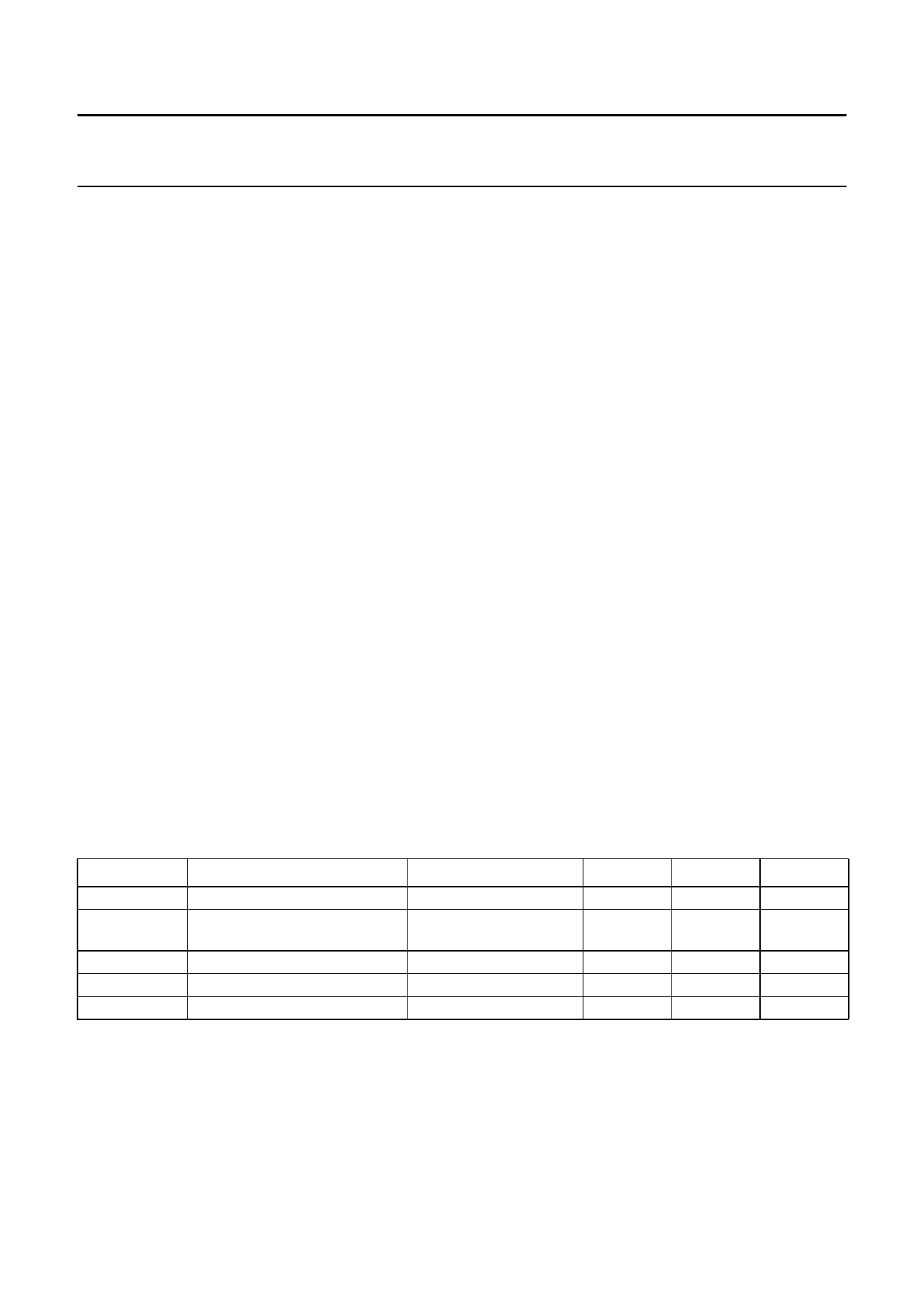
LIMITING VALUES
In accordance with the Absolute Maximum Rating System (IEC 134).
SYMBOL
VCC
Vn
Tamb
Tstg
Ves
PARAMETER
supply voltage
voltage at pins 1, 2 and 5 to 40
to pins 3 and 4
operating ambient temperature
storage temperature
electrostatic handling
CONDITIONS
note 1
MIN.
0
0
−40
−65
MAX.
10
VCC
+85
+150
UNIT
V
V
°C
°C
Note
1. Human body model: C = 100 pF; R = 1.5 kΩ; V ≥ 2 kV. Charge device model: C = 200 pF; R = 0 Ω; V ≥ 500 V.
1995 Dec 20
6
Share Link: 