TEA1541 Ver la hoja de datos (PDF) - Philips Electronics
Número de pieza
componentes Descripción
Fabricante
TEA1541 Datasheet PDF : 19 Pages
| |||
Philips Semiconductors
SMPS control IC with
synchronization function
Product specification
TEA1541
6.6 Minimum and maximum ‘on-time’
The minimum on-time of the converter is not limited by the
leading edge blanking time, and therefore can be zero.
The IC limits the maximum on-time to f--s---m-1---p---s-
where fsmps is the converter switching frequency in either
synchronized or unsynchronized mode. If the system
requires a longer on-time, a fault condition is assumed, for
example, if CVIN is removed, the IC will stop switching and
enter the safe restart mode.
6.7 Overvoltage protection
The TEA1541 allows OVP to be set accurately.
The flyback converter output voltage is accurately
represented by the voltage across the auxiliary winding.
The auxiliary winding voltage is monitored by the current
flowing into pin DEM during the demagnetizing cycle of the
transformer. The inevitable voltage spikes at pin DEM are
reduced using an internal filter.
If the output voltage causes the current into pin DEM to
exceed the OVP level lOVP(DEM), the OVP circuit turns off
the power MOSFET. The controller then waits until the
VCC(UVLO) condition is reached. This is followed by a safe
restart cycle, before switching recommences.
This process is repeated until the OVP condition ends.
The output voltage at which OVP activates, Vo(ovp) is set by
the value of resistor, RDEM, (see Fig.8) using the equation:
Vo(ovp) = N---N--a---us--x- × (IOVP(DEM) × RDEM + Vclamp(DEM)(pos))
where N is the number of turns on the transformer
windings; Vclamp(DEM)(pos) is the positive clamp voltage on
pin DEM; reference current IOVP(DEM) is set internally.
6.8 Overcurrent protection and overpower
protection
The current in the transformer primary is measured
accurately by the internal cycle-by-cycle source current
limit circuit using the external sense resistor Rsense.
The accuracy of the current limit circuit allows the
transformer core to have a minimum specification for the
output power required. The OCP circuit limits the ‘sense’
voltage to an internal level, and is activated after the
leading edge blanking period, tleb generated by the
Leading Edge Blanking circuit (LEB shown in Fig.2).
Leading edge blanking is required to inhibit OCP for a
short period when the power MOSFET turns on.
This ensures that the MOSFET is not turned off
prematurely due to the false sensing of an overcurrent
condition caused by current spikes produced by the
discharge of primary-side snubber and parasitic
capacitances.
The OCP level is adjusted proportionally to the switching
frequency such that the product of (Ipeak)2 × frequency
stays constant. This arrangement also implements OPP,
ensuring that the maximum output power is independent of
the switching frequency, otherwise the output power would
increase in direct proportion to the switching frequency.
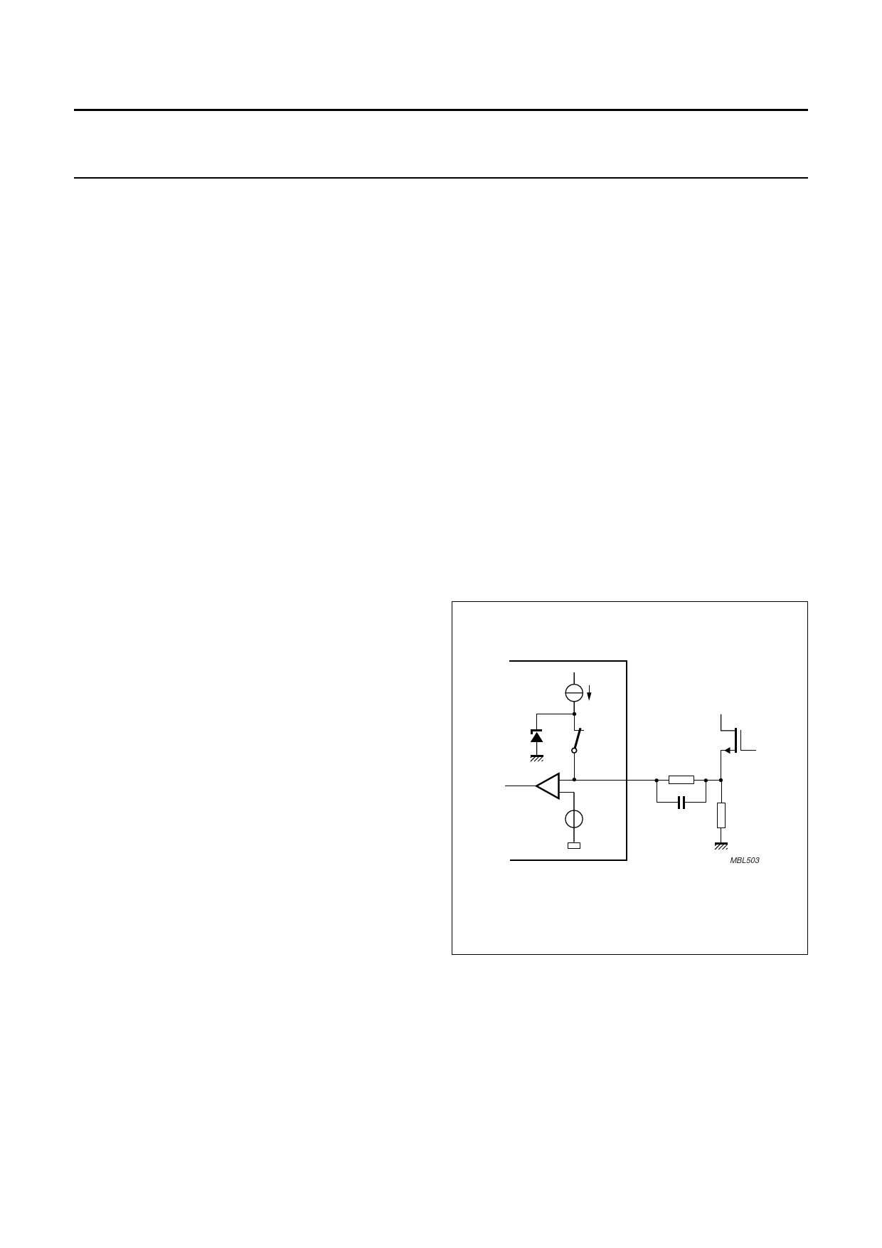
6.9 Soft start
The soft start function allows the transformer peak current
to slowly increase at every start-up and restart, to prevent
transformer rattle.
The soft start function requires a resistor RSS and
capacitor CSS to be connected between pin Isense and the
sense resistor Rsense (see Fig.7). CSS is charged by an
internal current source ISS to V = ISS × RSS, to a maximum
of approximately 0.5 V.
handbook, halfpage
0.5 V
ISS
start-up
5 Isense RSS
Vocp
CSS
Rsense
MBL503
Fig.7 Soft start.
The rate at which the primary current increases can be
adjusted by changing the values of RSS and CSS to change
the circuit time constant: τ = RSS × CSS
The maximum primary current is calculated by the
equation: Iprimary(max) = V-----s--e---n---s---e---(-m----a--R-x---)s--e-–--n--s(---eI--S---S----×-----R-----S---S---)-
2003 Aug 11
9
Share Link: 