TDF8599BTH Ver la hoja de datos (PDF) - NXP Semiconductors.
Número de pieza
componentes Descripción
Fabricante
TDF8599BTH
NXP Semiconductors.

TDF8599BTH Datasheet PDF : 54 Pages
| |||
NXP Semiconductors
TDF8599B
I2C-bus controlled dual channel class-D power amplifier
The TDF8599B includes integrated common circuits for all channels such as the oscillator,
all reference sources, mode functionality and a digital timing manager. In addition, the
built-in protection includes thermal foldback, temperature, overcurrent and overvoltage
(load dump).
The TDF8599B operates in either I2C-bus mode or non-I2C-bus mode. In I2C-bus mode,
DC load detection, frequency hopping and extended configuration functions are provided
together with enhanced diagnostic information.
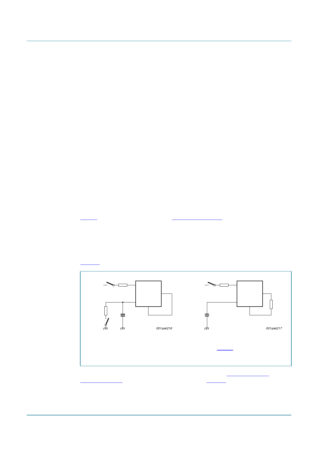
8.2 Mode selection
The mode pins EN, ADS and SEL_MUTE enable mute state, I2C-bus mode and Operating
mode switching.
Pin SEL_MUTE is used to mute and unmute the device and must be connected to an
external capacitor (CON). This capacitor generates a time constant which is used to
ensure smooth fade-in and fade-out of the input signal.
The TDF8599B is enabled when pin EN is HIGH. When pin EN is LOW, the TDF8599B is
off and the supply current is at its lowest value (typically 2 µA). When off, the TDF8599B is
completely deactivated and will not react to I2C-bus commands.
I2C-bus mode is selected by connecting a resistor between pins ADS and AGND. In
I2C-bus mode with pin EN HIGH, the TDF8599B waits for further commands (see
Table 4). I2C-bus mode is described in Section 9 on page 23.
Non-I2C-bus mode is selected by connecting pin ADS to pin AGND. In non-I2C-bus mode,
the default TDF8599B state is Mute mode. The amplifiers switch idle (50 % duty cycle)
and the audio signal is suppressed at the output. In addition, the capacitor (CSVRR) is
charged to half the supply voltage. To enter Operating mode, pin SEL_MUTE must be
HIGH with S1 open, enabling capacitor (CON) charged by an internal pull-up (see
Figure 3). In addition, pin EN must be driven HIGH.
3.3 V
S2
EN
ADS
TDF8599B
SEL_MUTE
CON
S1
AGND
001aak216
3.3 V
S2
EN
ADS
TDF8599B
SEL_MUTE
AGND
RADS
CON
001aak217
a. Non-I2C-bus mode
Fig 3. Mode selection
b. I2C-bus mode
See Table 13 for detailed information on
RADS.
I2C-bus mode and non-I2C-bus mode control are described in Table 4 on page 7 and
Table 5 on page 7. Switches S1 and S2 are shown in Figure 3.
TDF8599B_1
Product data sheet
Rev. 01 — 29 July 2009
© NXP B.V. 2009. All rights reserved.
6 of 54
Share Link: