TDA7490SA Ver la hoja de datos (PDF) - STMicroelectronics
Número de pieza
componentes Descripción
Fabricante
TDA7490SA Datasheet PDF : 13 Pages
| |||
TDA7490SA
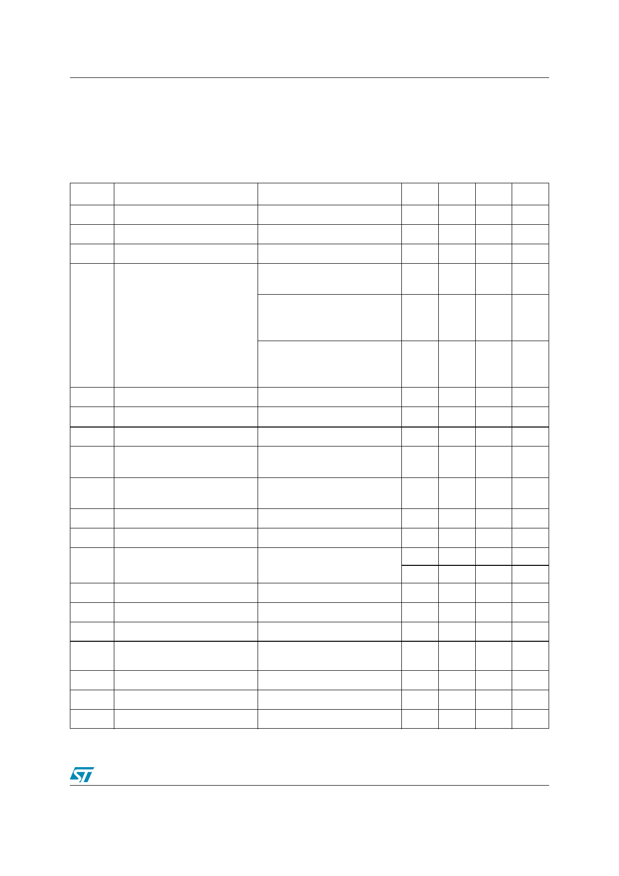
2 Electrical characteristcs
2 Electrical characteristcs
Table 3.
electrical characteristcs (Refer to the test circuit, VCC = ±13.5V; RL = 8Ω;
Demod. filter L = 33 µH, C = 220nF; f = 1KHz; R1 = 27kΩ; Tamb = 25°C unless otherwise
specified.)
Symbol
Parameter
Test Condition
Min. Typ. Max. Unit
VS Supply Range
Iq Total Quiescent Current
VOS Output Offset Voltage
Po Output Power
PD
h
THD
Imax
Tj
Maximum Dissipated Power
Efficiency (1)
Total Harmonic Distortion
Overcurrent Protection
Threshold
Thermal Shut-down Junction
Temperature
RL = ∞; no LC filter
THD = 10%
THD = 1%
VCC = ±10V; RL = 4Ω
THD = 10%
THD = 1%
VCC = ±6V; RL = 4Ω
THD = 10%
THD = 1%
Po = 10+10W; THD = 10%
Po = 10+10W; RL = 8Ω
RL = 8Ω; Po = 0.5W
RL = 0
±7
±15
V
60
mA
-150
+150 mV
10
W
8.2
W
10
W
8
W
4
W
3
W
3.5
W
86
%
0.1
%
2
2.5
A
150
°C
GV Closed Loop Gain
∆GV Gain Matching
eN Total Input Noise
A Curve
f = 20Hz to 22KHz
CT
Ri
SVR
Vrmax
Tr, Tf
RDSON
FSW
Cross Talk
Input Resistance
Supply Voltage Rejection
Overvoltage Protection
Threshold
Rising and Falling Time
Power Transistor on Resistance
Switching Frequency
f = 1KHz
f = 100Hz; Vr = 0.5
Internal Oscillator
30
dB
-1
1
dB
7
µV
12
µV
t.b.d.
dB
30
kΩ
60
dB
30
V
50
ns
0.3
W
180 200 220 KHz
5/13
Share Link: 