TDA6403AM/C1 Ver la hoja de datos (PDF) - Philips Electronics
Número de pieza
componentes Descripción
Fabricante
TDA6403AM/C1
Philips Electronics

TDA6403AM/C1 Datasheet PDF : 40 Pages
| |||
Philips Semiconductors
5 V mixers/oscillators and synthesizers for
cable TV and VCR 2-band tuners
Product specification
TDA6402; TDA6402A;
TDA6403; TDA6403A
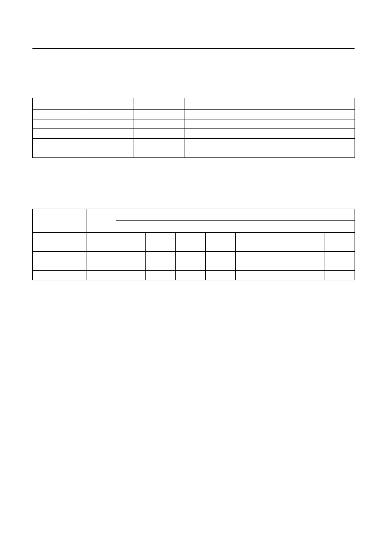
Table 11 A to D converter levels (note 1)
A2
A1
A0
1
0
0
0
1
1
0
1
0
0
0
1
0
0
0
Note
1. Accuracy is ±0.03 × VCC.
POWER-ON RESET
Table 12 Default bits at power-on reset
NAME
BYTE
MSB
Address byte
ADB
1
1
Divider byte 1
DB1
0
X
Divider byte 2
DB2
X
X
Control byte
CB
1
1
Band switch byte
BB
X
X
VOLTAGE APPLIED ON ADC INPUT
0.60 × VCC to 1.00 × VCC
0.45 × VCC to 0.60 × VCC
0.30 × VCC to 0.45 × VCC
0.15 × VCC to 0.30 × VCC
0 to 0.15 × VCC
BITS
LSB
0
0
0
MA1
MA0
X
X
X
X
X
X
X
X
X
X
X
X
X
0
0
1
X
1
1
X
X
0
0
0
0
The power-on detection threshold voltage VPOR is set to
VCC = 2 V at room temperature. Below this threshold, the
device is reset to the power-on state.
At power-on state, the charge pump current is set to
280 µA, the tuning voltage output is disabled, the test bits
T2, T1 and T0 are set to ‘001’ (automatic charge pump
switch ‘ON’) and RSB is set to logic 1.
PUHF is ‘OFF’, which means that the UHF oscillator and
the UHF mixer are switched off. Consequently, the VHF
oscillator and the VHF mixer are switched on. PVHFL and
PVHFH are ‘OFF’, which means that the VHF tank circuit
is working in the VHF I sub-band. The tuning amplifier is
switched off until the first transmission. In that case, the
tank circuit in VHF I is supplied with the maximum tuning
voltage. The oscillator is therefore working at the end of
the VHF I sub-band.
3-wire bus mode (SW = OPEN or VCC)
During a HIGH-level on the CE input (enable line), the data
is clocked into the data register at the HIGH-to-LOW
transition of the clock. The first four bits control the PNP
ports and are loaded into the internal band switch register
on the 5th rising edge of the clock pulse. The frequency
bits are loaded into the frequency register at the
HIGH-to-LOW transition of the chip enable line when an
18-bit or 19-bit data word is transmitted (see Figs 4 and 5).
When a 27-bit data word is transmitted, the frequency bits
are loaded into the frequency register on the 20th rising
edge of the clock pulse and the control bits at the
HIGH-to-LOW transition of the chip enable line (see Fig.6).
In this mode, the reference divider is given by the RSA and
RSB bits (see Table 8). The test bits T2, T1 and T0, the
charge pump bit CP, the ratio select bit RSB and the OS
bit can only be selected or changed with a 27-bit
transmission. They remain programmed if an 18-bit or
19-bit transmission occurs. Only RSA is controlled by the
transmission length when the 18-bit or 19-bit format is
used. When an 18-bit data word is transmitted, the most
significant bit of the divider N14 is internally set to logic 0
and the RSA bit is set to logic 1. When a 19-bit data word
is transmitted, the RSA bit is set to logic 0.
A data word of less than 18 bits will not affect the
frequency register of the device. The definition of the bits
is unchanged compared to I2C-bus mode.
It is not allowed to address the devices with words whose
length is different from 18, 19 or 27 bits.
2000 Jan 24
11
Share Link: