TC2001 Ver la hoja de datos (PDF) - Tripath Technology Inc.
Número de pieza
componentes Descripción
Fabricante
TC2001
Tripath Technology Inc.

TC2001 Datasheet PDF : 34 Pages
| |||
Tripath Technology, Inc. - Technical Information
Note 11: These supply voltages are calculated using the IVPPSENSE and IVNNSENSE values shown in the
Electrical Characteristics table. The typical voltage values shown are calculated using a RVPP and RVNN
values without any tolerance variation. The minimum and maximum voltage limits shown include either a
+1% or –1% (+1% for Over-voltage turn on and Under-voltage turn off, -1% for Over-voltage turn off and
Under-voltage turn on) variation of RVPP or RVNN off the nominal 357kohm, 324kohm, and 976kohm
values. These voltage specifications are examples to show both typical and worst case voltage ranges for
the given RVPP and RVNN resistor values. Please refer to the Application Information section for a more
detailed description of how to calculate the over and under voltage trip voltages for a given resistor value.
Note 12: The fact that the over-voltage turn on specifications exceed the absolute maximum of +/-60V for the TK2150
does not imply that the part will work at these elevated supply voltages. It also does not imply that the
TK2150 is tested or guaranteed at these supply voltages. The supply voltages are simply a calculation
based on the process spread of the IVPPSENSE and IVNNSENSE currents (see note 7). The supply
voltage must be maintained below the absolute maximum of +/-60V or permanent damage to the TK2150
may occur.
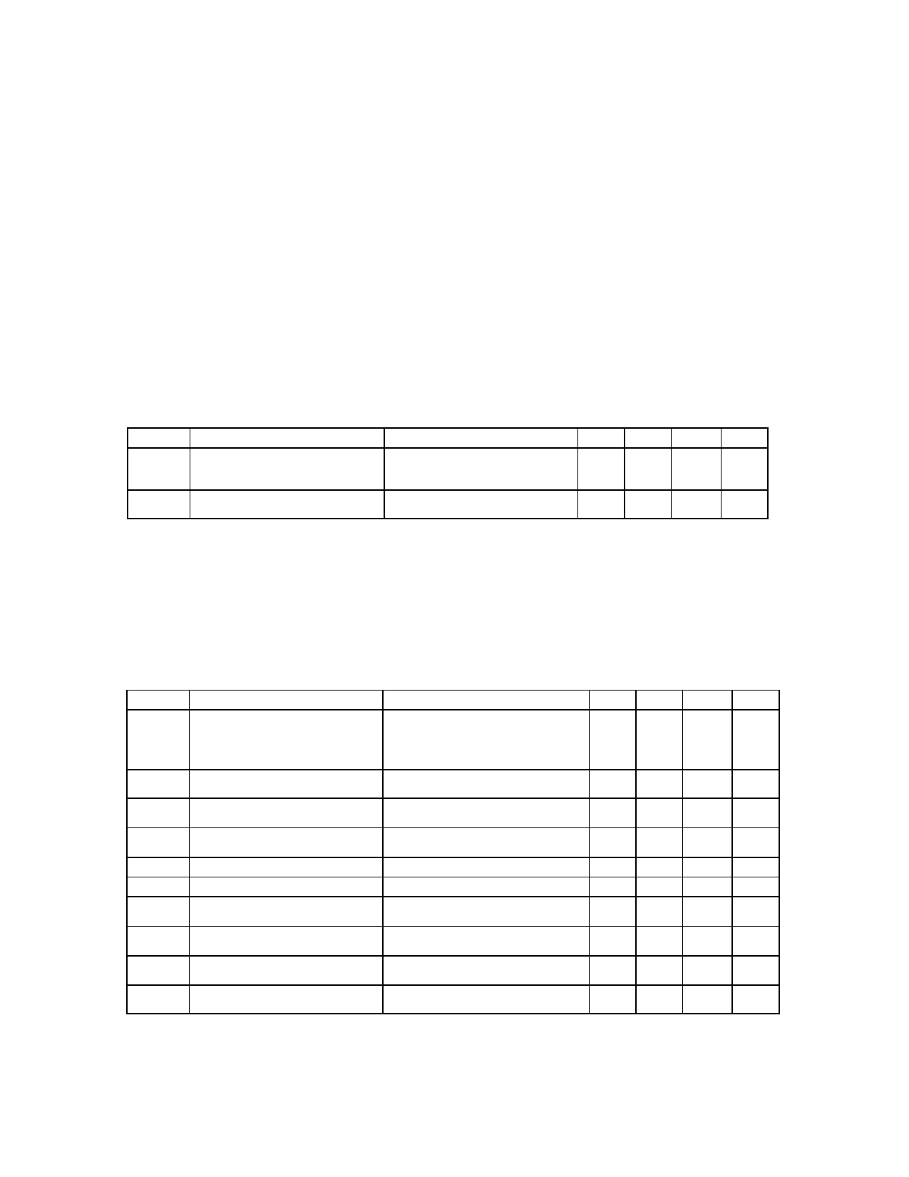
Electrical Characteristics TP2150 (Note 13)
TA = 25 °C. See Application/Test Circuit on page 7. Unless otherwise noted, the supply voltage is
VPP=|VNN|=45V.
SYMBOL
PARAMETER
Iq
IMUTE
Quiescent Current
(No load, BBM0=1,BBM1=0,
Mute = 0V)
Mute Supply Current
(No load, Mute = 5V)
CONDITIONS
VPP = +45V
VNN = -45V (Note 14)
VPP = +45V
VNN = -45V
MIN.
TYP.
25
45
1
1
MAX.
UNITS
mA
mA
mA
mA
Note 13: Minimum and maximum limits are guaranteed but may not be 100% tested.
Note 14: The difference in the VPP and VNN current draw is due to the VN10 regulator sourcing current to the
VNN supply.
Performance Characteristics TK2150 – Single Ended
TA = 25 °C. Unless otherwise noted, the supply voltage is VPP=|VNN|=45V, the input frequency is 1kHz
and the measurement bandwidth is 20kHz. See Application/Test Circuit.
SYMBOL
PARAMETER
POUT
Output Power
(continuous RMS/Channel)
THD + N Total Harmonic Distortion Plus
Noise
IHF-IM IHF Intermodulation Distortion
SNR
Signal-to-Noise Ratio
CS
Channel Separation
η
Power Efficiency
AV
Amplifier Gain
AVERROR Channel to Channel Gain Error
eNOUT
VOFFSET
Output Noise Voltage
Output Offset Voltage
CONDITIONS
THD+N = 0.1%, RL = 8Ω
RL = 6Ω
THD+N = 1%, RL = 8Ω
RL = 6Ω
POUT = 70W/Channel, RL = 8Ω
19kHz, 20kHz, 1:1 (IHF), RL = 8Ω
POUT = 30W/Channel
A Weighted, RL = 6Ω,
POUT = 155W/Channel
0dBr = 30W, RL = 8Ω, f = 1kHz
POUT = 150W/Channel, RL = 8Ω
POUT = 10W/Channel, RL = 6Ω
See Application / Test Circuit
POUT = 10W/Channel, RL = 6Ω
See Application / Test Circuit
A Weighted, no signal, input shorted,
DC offset nulled to zero, RFBC = 11kΩ
No Load, Mute = Logic Low
0.1% RFBA, RFBB, RFBC resistors
MIN.
-1.0
TYP.
100
135
120
155
0.012
0.02
104.5
92
93
13.3
180
MAX.
UNITS
W
W
W
W
%
%
dB
dB
%
V/V
0.5
dB
µV
1.0
V
4
TK2150 – Rev. 1.0/12.02
Share Link: