TC2014 Ver la hoja de datos (PDF) - Microchip Technology
Número de pieza
componentes Descripción
Fabricante
TC2014 Datasheet PDF : 20 Pages
| |||
5.0 THERMAL CONSIDERATIONS
5.1 Thermal Shutdown
Integrated thermal protection circuitry shuts the regula-
tor off when the die temperature exceeds approxi-
mately 160°C. The regulator remains off until the die
temperature cools to approximatley 150°C.
5.2 Power Dissipation
The amount of power the regulator dissipates is primar-
ily a function of input voltage, output voltage and output
current.
The following equation is used to calculate worst-case
power dissipation.
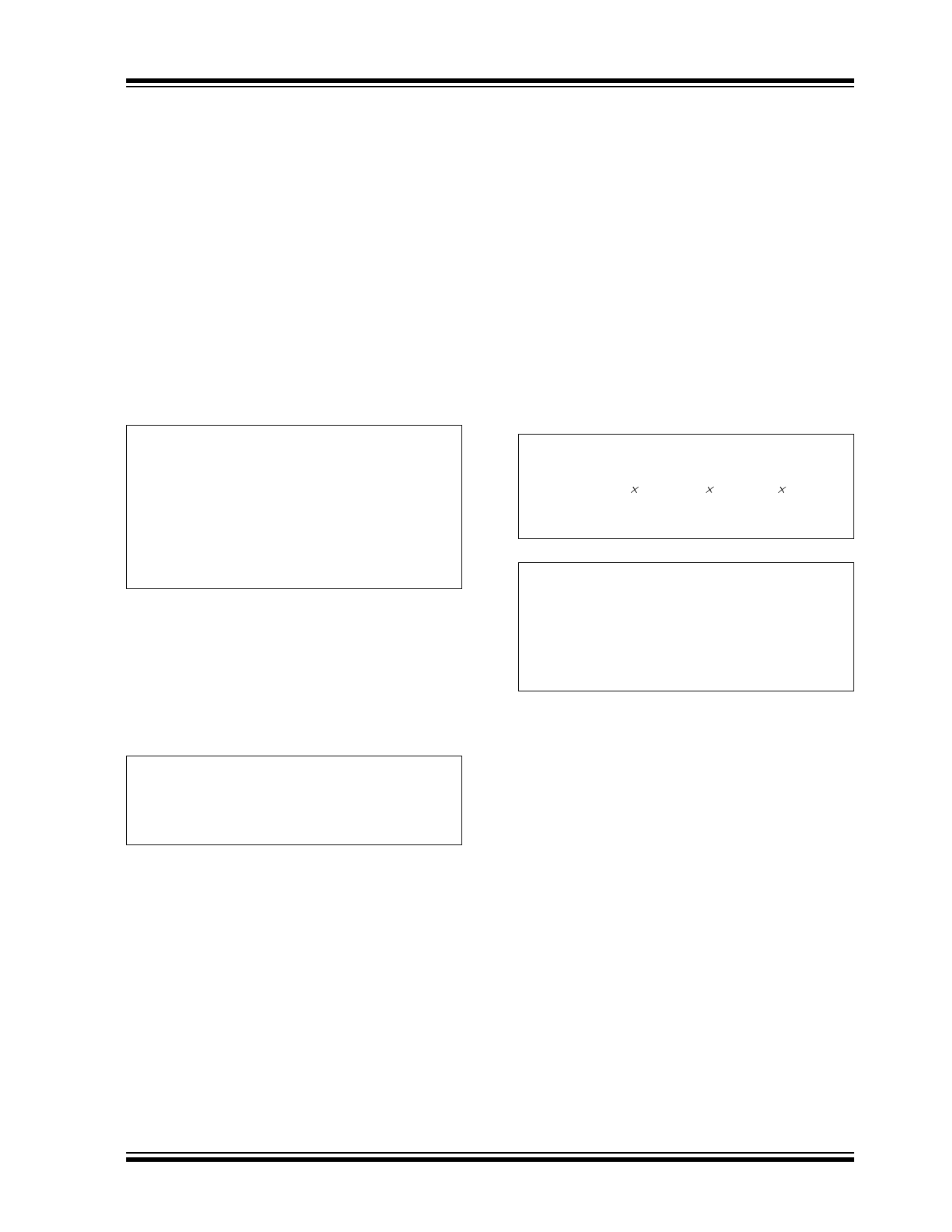
EQUATION 5-1:
PD VINMAX – VOUTMINILMAX
Where:
PD
= Worst-case actual power dissipation
VINMAX = Maximum voltage on VIN
VOUTMIN = Minimum regulator output voltage
ILMAX = Maximum output (load) current
The maximum allowable power dissipation (PDMAX) is
a function of the maximum ambient temperature
(TAMAX), the maximum allowable die temperature
(TJMAX) (+125°C) and the thermal resistance from junc-
tion-to-air (JA). The 5-Pin SOT-23A package has a JA
of approximately 220°C/Watt when mounted on a
typical two-layer FR4 dielectric copper-clad PC board.
EQUATION 5-2:
PDMAX = T----J---M----A---X----–-J---A-T---A----M----A---X-
Where all terms are previously defined.
TC2014/2015/2185
The PD equation can be used in conjunction with the
PDMAX equation to ensure that regulator thermal
operation is within limits. For example:
Given:
VINMAX
VOUTMIN
ILOADMAX
TJMAX
TAMAX
= 3.0V +10%
= 2.7V – 2.5%
= 40 mA
= +125°C
= +55°C
Find:
1. Actual power dissipation
2. Maximum allowable dissipation
Actual power dissipation:
PD = VINMAX – VOUTMINILMAX
= 3.0 1.1 – 2.7 0.97540 10–3
= 26.7mW
Maximum allowable power dissipation:
PDMAX = T----J--M-----A---X----–-J---A-T---A----M----A---X-
= 1----2---5----–-----5---5-
220
= 318mW
In this example, the TC2014 dissipates a maximum of
only 26.7 mW; far below the allowable limit of 318 mW.
In a similar manner, the PD and PDMAX equations can
be used to calculate maximum current and/or input
voltage limits.
5.3 Layout Considerations
The primary path of heat conduction out of the package
is via the package leads. Therefore, layouts having a
ground plane, wide traces at the pads and wide power
supply bus lines combine to lower JA and, therefore,
increase the maximum allowable power dissipation
limit.
2001-2012 Microchip Technology Inc.
DS21662F-page 11
Share Link: 