TC1121 Ver la hoja de datos (PDF) - Microchip Technology
Número de pieza
componentes Descripción
Fabricante
TC1121 Datasheet PDF : 14 Pages
| |||
TC1121
1.0 ELECTRICAL
CHARACTERISTICS
Absolute Maximum Ratings*
Supply Voltage (VDD) ............................................... 6V
OSC, FC, SHDN Input Voltage .....-0.3V to (V+ + 0.3V)
Output Short Circuit Duration ........................... 10 Sec.
Package Power Dissipation (TA ≤ 70°C)
8-Pin PDIP .............................................. 730 mW
8-Pin SOIC .............................................. 470 mW
8-Pin MSOP ............................................ 333 mW
Operating Temperature Range
C Suffix............................................ 0°C to +70°C
E Suffix......................................... -40°C to +85°C
Storage Temperature Range.............. -65°C to +150°C
*Stresses above those listed under “Absolute
Maximum Ratings” may cause permanent damage to
the device. These are stress ratings only and functional
operation of the device at these or any other conditions
above those indicated in the operation sections of the
specifications is not implied. Exposure to Absolute
Maximum Rating conditions for extended periods may
affect device reliability.
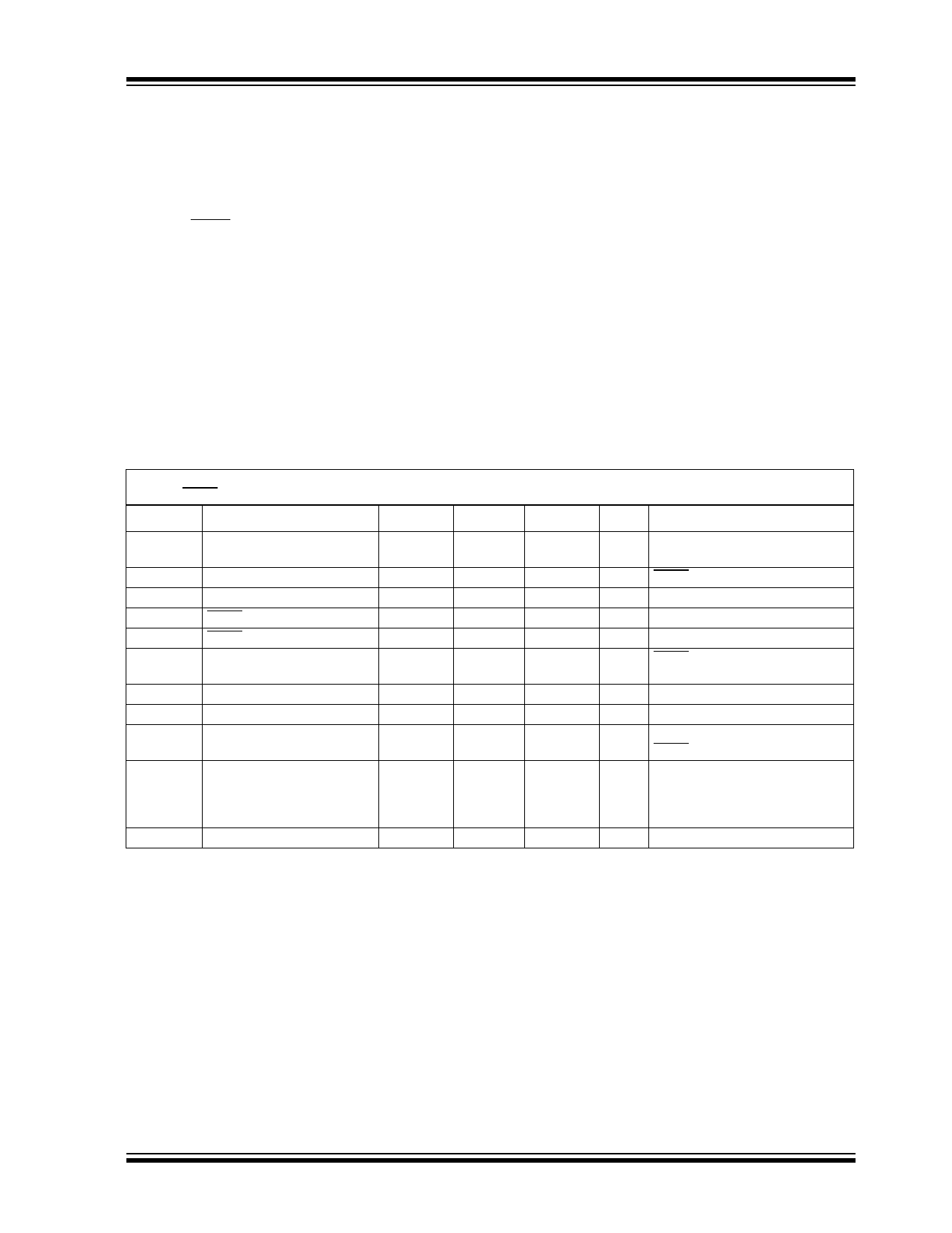
TC1121 ELECTRICAL SPECIFICATIONS
Electrical Characteristics: TA = 0°C to 70°C (C suffix), -40°C to +85°C (E suffix), V+= 5V ±10% COSC = Open, C1, C2 = 10 μF,
FC = V+, SHDN = VIH, typical values are at TA = 25°C unless otherwise noted.
Symbol
Parameter
Min
Typ
Max
Units
Test Conditions
IDD
Active Supply Current
ISHUTDOWN Shutdown Supply Current
V+
Supply Voltage
—
50
100
μA RL = Open, FC = Open or GND
—
0.6
1
mA RL = Open, FC = V+
—
0.2
1.0
μA SHDN = 0V
2.4
—
5.5
V
VIH
SHDN Input Logic High
VDD x 0.8
—
—
V
VIL
SHDN Input Logic Low
—
—
0.4
V
IIN
Input Leakage Current
-1
—
-4
—
1
μA SHDN, OSC
4
FC pin
ROUT
IOUT
FOSC
PEFF
VEFF
Note 1:
Output Source Resistance
—
12
20
Ω IOUT = 60 mA
Output Current
60
100
VOUT = more negative than -3.75V
Oscillator Frequency
5
10
100
200
—
kHz Pin 7 Open, Pin 1 Open or GND
—
SHDN = VIH, Pin 1 = V+
Power Efficiency
—
—
—
% FC = GND for all
93
97
—
RL = 2k between V+ and VOUT
94
97
—
RL = 1kΩ between VOUT and GND
—
92
IL = 60 mA to GND
Voltage Conversion Efficiency
99
99.9
—
% RL = Open
Connecting any input terminal to voltages greater than V+ or less than GND may cause destructive latch-up. It is recommended that no
inputs from sources operating from external supplies be applied prior to “power up” of the TC1121.
© 2006 Microchip Technology Inc.
DS21358C-page 3
Share Link: 