TC1017 Ver la hoja de datos (PDF) - Microchip Technology
Número de pieza
componentes Descripción
Fabricante
TC1017 Datasheet PDF : 22 Pages
| |||
TC1017
4.0 DETAILED DESCRIPTION
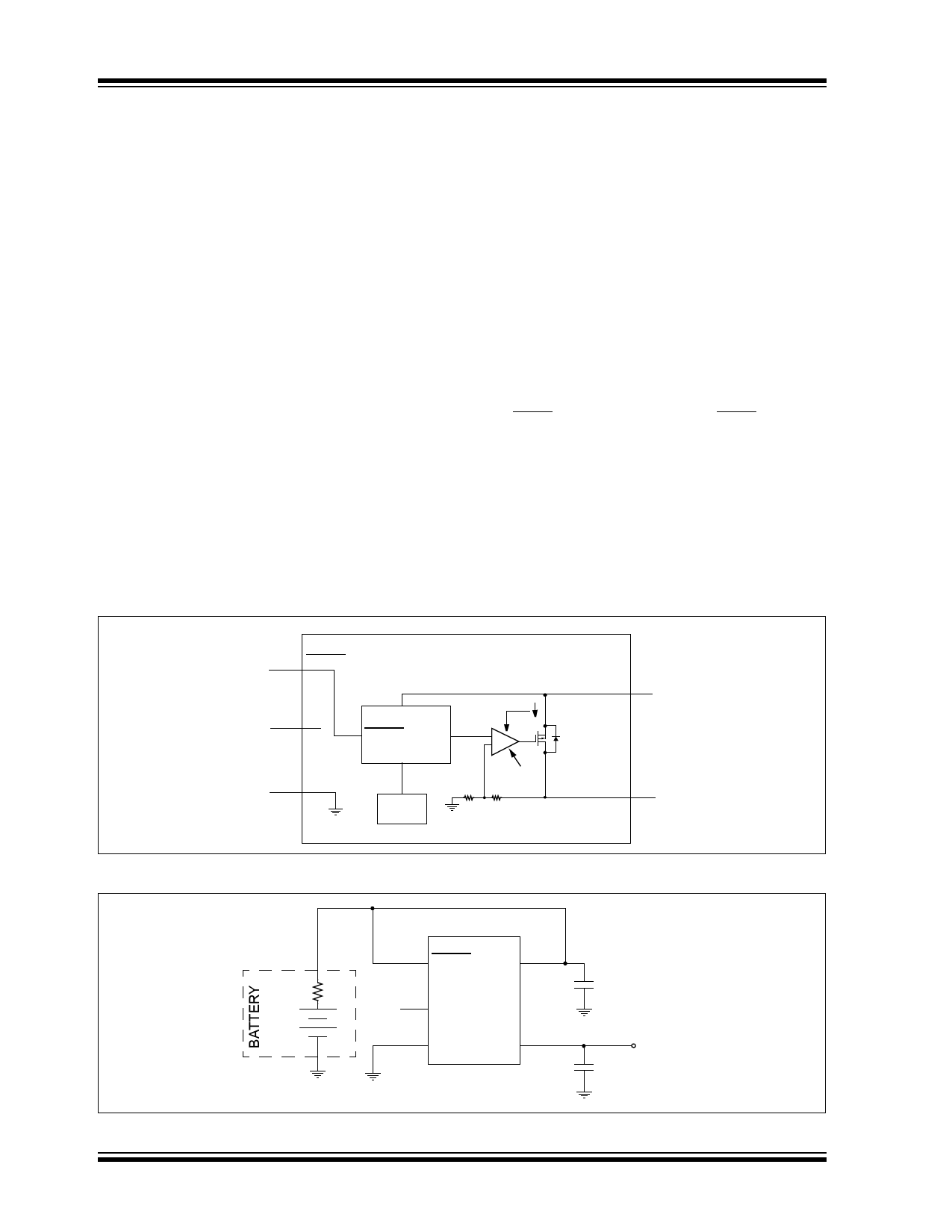
The TC1017 is a precision, fixed-output, linear voltage
regulator. The internal linear pass element is a
P-Channel MOSFET. As with all P-Channel CMOS
LDOs, there is a body drain diode with the cathode
connected to VIN and the anode connected to VOUT
(Figure 4-1).
As is shown in Figure 4-1, the output voltage of the
LDO is sensed and divided down internally to reduce
external component count. The internal error amplifier
has a fixed bandgap reference on the inverting input
and the sensed output voltage on the non-inverting
input. The error amplifier output will pull the gate
voltage down until the inputs of the error amplifier are
equal to regulate the output voltage.
By sensing the current in the P-Channel MOSFET, the
maximum current delivered to the load is limited to a
typical average value of 120 mA, preventing excessive
current from damaging the printed circuit board in the
event of a shorted or faulted load.
An internal thermal sensing device is used to monitor
the junction temperature of the LDO. When the sensed
temperature is over the set threshold of 160°C (typical),
the P-Channel MOSFET is turned off. When the
P-Channel is off, the power dissipation internal to the
device is almost zero. The device cools until the
junction temperature is approximately 150°C and the
P-Channel is turned on. If the internal power dissipation
is still high enough for the junction to rise to 160°C, it
will again shut off and cool. The maximum operating
junction temperature of the device is 125°C. Steady-
state operation at or near the 160°C overtemperature
point can lead to permanent damage of the device.
The output voltage VOUT remains stable over the entire
input operating voltage range (2.7V to 6.0V) and the
entire load range (0 mA to 150 mA). The output voltage
is sensed through an internal resistor divider and
compared with a precision internal voltage reference.
Several fixed-output voltages are available by
changing the value of the internal resistor divider.
Figure 4-2 shows a typical application circuit. The
regulator is enabled any time the shutdown input pin is
at or above VIH. It is shut down (disabled) any time the
shutdown input pin is below VIL. For applications where
the SHDN feature is not used, tie the SHDN pin directly
to the input supply voltage source. While in shutdown,
the supply current decreases to 0.006 µA (typical) and
the P-Channel MOSFET is turned off.
As shown in Figure 4-2, batteries have internal source
impedance. An input capacitor is used to lower the
input impedance of the LDO. In some applications, high
input impedance can cause the LDO to become
unstable. Adding more input capacitance can
compensate for this.
FIGURE 4-1:
1 SHDN
2 NC
3 GND
Current Limit
VIN
SHDN VREF
Control
+-EA
VIN 5
Body
Diode
Over
Temp.
Error
Amp
R1 R2
Feedback Resistors
VOUT 4
TC1017 Block Diagram.
RSOURCE
1 SHDN VIN 5
TC1017
CIN
2 NC
3 GND
VOUT 4
COUT
1 µF Ceramic
Load
1 µF Ceramic
FIGURE 4-2:
Typical Application Circuit.
DS21813B-page 10
2003 Microchip Technology Inc.
Share Link: 