TA8221 Ver la hoja de datos (PDF) - Toshiba
Número de pieza
componentes Descripción
Fabricante
TA8221 Datasheet PDF : 16 Pages
| |||
TA8221AHQ / ALQ
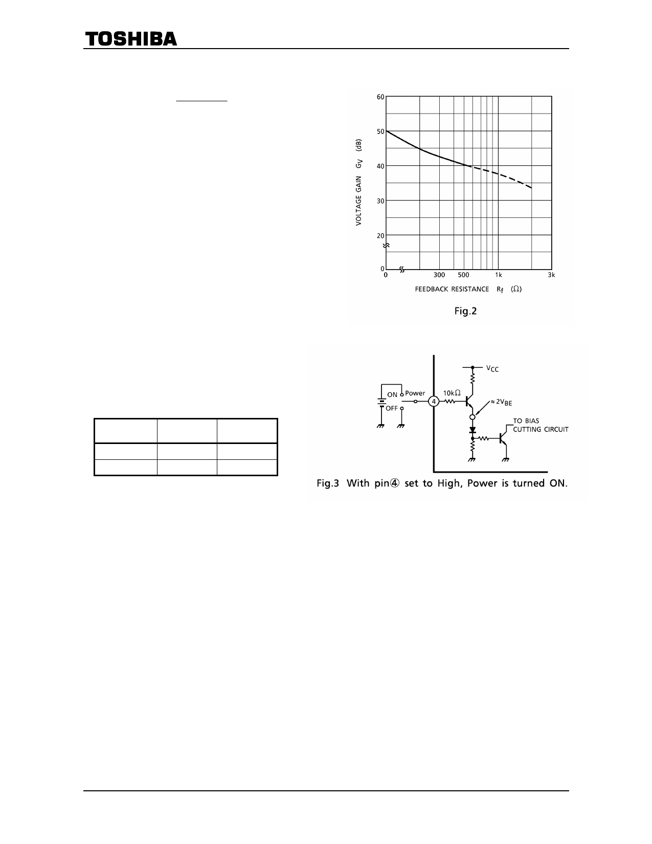
The total closed loop gain GV of this IC can be obtained by expression below when the closed loop voltage gain of
amp 1 is GV1.
GV1
=
20 l og
R1+ (Rf + R2)
Rf + R2
(dB)
.....
(1)
The closed loop voltage gain of power amp, amp 3
and amp 4 is fixed at GV3≒GV4 = 20dB.
Therefore, the total closed circuit voltage gain GV is
obtained through BTL connection by the expression
below.
GV = GV1 + GV3 + 6 (dB) ............... (2)
For example, when Rf = 0Ω, GV is obtained by the
expressions (1) and (2) as shown below.
GV≒24 + 20 + 6 = 50dB
The voltage gain is reduced when Rf is increased. (Fig.2)
With the voltage gain reduced, since (1) the oscillation
stability is reduced, and (2) the pop noise changes when
VCC is set to on, refer to the items 3 and 4.
2. Stand−by SW function
By means of controlling pin(4) (stand−by terminal) to high
and low, the power suply can be set to on and off.
The threshold voltage of pin(4) is set at 2.1V (3VBE.),
and the power supply current is about 100µA (typ.) at the
stand−by state.
Control voltage of pin(4): V (SB)
Stand−by
Power
V (SB) (V)
On
Off
0~2
Off
On
3~VCC
Advantage of stand−by SW
(1) Since VCC can directly be controlled to on / off by the microcomputer, the switching relay can be omitted.
(2) Since the control current is microscopic, the switching relay of small current capacity is satisfactory for
switching.
3
2006-04-28
Share Link: 