TA8276HQ Ver la hoja de datos (PDF) - Toshiba
NГғmero de pieza
componentes DescripciГіn
Fabricante
TA8276HQ Datasheet PDF : 14 Pages
| |||
TA8276HQ
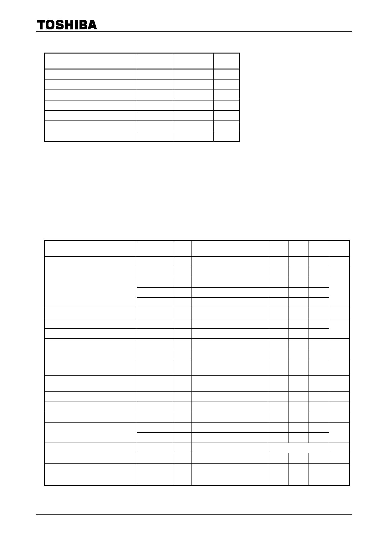
Maximum Ratings (Ta = 25В°C)
Characteristics
Symbol
Rating
Unit
Peak supply voltage (0.2 s)
DC supply voltage
Operation supply voltage
Output current (peak)
Power dissipation
Operation temperature
Storage temperature
VCC (surge)
50
V
VCC (DC)
25
V
VCC (opr)
18
V
IO (peak)
9
A
PD (Note 5)
125
W
Topr
в€’40~85
В°C
Tstg
в€’55~150
В°C
Note 5: Package thermal resistance Оёj-T = 1В°C/W (typ.)
(Ta = 25В°C, with infinite heat sink)
The absolute maximum ratings of a semiconductor device are a set of specified parameter values, which must not
be exceeded during operation, even for an instant. If any of these rating would be exceeded during operation, the
device electrical characteristics may be irreparably altered and the reliability and lifetime of the device can no
longer be guaranteed. Moreover, these operations with exceeded ratings may cause break down, damage and/or
degradation to any other equipment. Applications using the device should be designed such that each maximum
rating will never be exceeded in any operating conditions. Before using, creating and/or producing designs, refer to
and comply with the precautions and conditions set forth in this documents.
Electrical Characteristics
(unless otherwise specified, VCC = 13.2 V, f = 1 kHz, RL = 4 Ω, Ta = 25°C)
Characteristics
Quiescent current
Output power
Total harmonic distortion
Voltage gain
Voltage gain ratio
Output noise voltage
Ripple rejection ratio
Cross talk
Output offset voltage
Input resistance
Stand-by current
Stand-by control voltage
Mute control voltage
Mute attenuation
Symbol
Test
Circuit
Test Condition
ICCQ
вҺҮ VIN = 0
POUT MAX (1) вҺҮ VCC = 14.4 V, max Power
POUT MAX (2) вҺҮ VCC = 13.7 V, max Power
POUT (1)
вҺҮ VCC = 14.4 V, THD = 10%
POUT (2)
вҺҮ THD = 10%
THD
вҺҮ POUT = 5 W
GV
вҺҮ VOUT = 0.775 Vrms (0 dBm)
∆GV
вҺҮ VOUT = 0.775 Vrms (0 dBm)
VNO (1)
вҺҮ Rg = 0 Ω, DIN45405
VNO (2)
вҺҮ Rg = 0 Ω, BW = 20 Hz~20 kHz
R.R.
вҺҮ
frip = 100 Hz, Rg = 620 Ω
Vrip = 0.775 Vrms (0 dBm)
C.T.
вҺҮ
Rg = 620 Ω
VOUT = 0.775 Vrms (0 dBm)
VOFFSET
вҺҮ
вҺҮ
RIN
вҺҮ
вҺҮ
ISB
вҺҮ Stand-by condition
VSB H
вҺҮ Power: ON
VSB L
вҺҮ Power: OFF
(Note 2)
VM H
VM L
вҺҮ Mute: OFF
вҺҮ Mute: ON, R1 = 10 kΩ
ATT M
Mute: ON,
вҺҮ VOUT = 7.75 Vrms (20 dBm) at
Mute: OFF.
Min
вҺҮ
вҺҮ
вҺҮ
вҺҮ
17
вҺҮ
24
в€’1.0
вҺҮ
вҺҮ
40
вҺҮ
в€’150
вҺҮ
вҺҮ
3.0
0
0
80
Typ.
200
35
31
23
20
0.02
26
0
0.12
0.10
50
65
0
90
2
вҺҮ
вҺҮ
Open
вҺҮ
90
Max Unit
400 mA
вҺҮ
вҺҮ
W
вҺҮ
вҺҮ
0.2
%
28
dB
1.0
вҺҮ
mVrms
0.35
вҺҮ
dB
вҺҮ
dB
150 mV
вҺҮ
kΩ
10
ВµA
VCC
V
1.5
вҺҮ
0.5
V
вҺҮ
dB
Note 2: Muting function have to be controlled by open and low logic, which logic is a transistor, FET and Вµ-COM port
of IMUTE > 250 ВµA ability.This means than the mute control terminal : pin 22 must not be pulled-up.
8
2004-05-10
Share Link: 