TA4003F Ver la hoja de datos (PDF) - Toshiba
Número de pieza
componentes Descripción
Fabricante
TA4003F Datasheet PDF : 5 Pages
| |||
TA4003F
Electrical Characteristics (Ta = 25°C) (Note2)
Characteristics
Circuit current
Insertion gain
Band width
Noise figure
Input return loss
Output return loss
Isolation
Maximum output level
Symbol
ICC
|S21|2
BW
NF
|S11|2
|S22|2
|S12|2
PO
Test
Circuit
Test Condition
Min
― VCC = 2 V, non carrier
2.5
1 VCC = 2 V, f = 500 MHz
9
1 VCC = 2 V
(Note 3) 1.2
1 VCC = 2 V, f = 500 MHz
―
1 VCC = 2 V, f = 500 MHz
―
1 VCC = 2 V, f = 500 MHz
―
1 VCC = 2 V, f = 500 MHz
―
1
VCC = 2 V, f = 500 MHz,
Pin = 0dBmW
―
Typ.
3.5
11
1.5
5.2
−7.5
−7.5
−24
0
Max Unit
4.5 mA
14
dB
― GHz
7
dB
―
dB
―
dB
―
dB
― dBmW
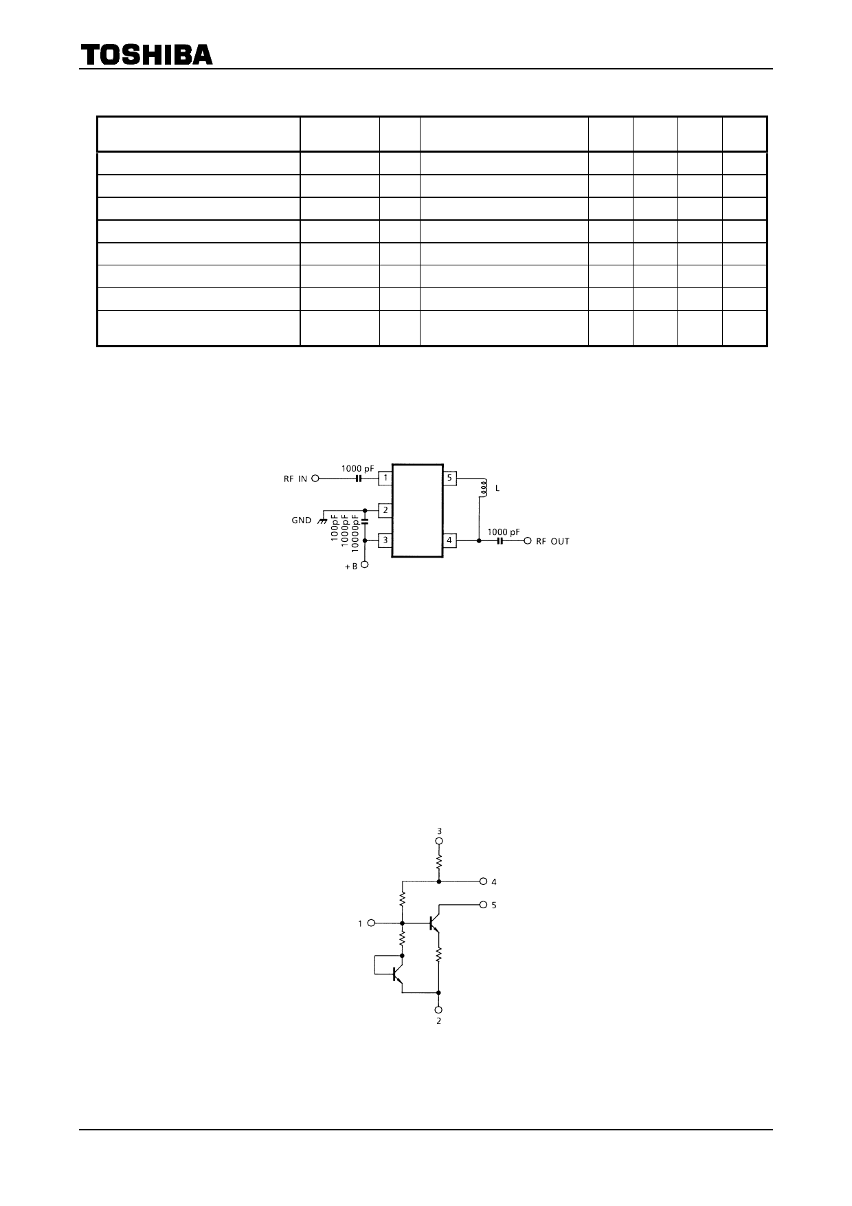
Note 2: Have use for connect inductance between terminal 4 and 5 8 nH at VCC = 2 V
Note 3: BW is frequency of 3dB down from |S21|2 at 500 MHz.
Test Circuit 1 (top view)
Notice
The circuits and measurements contained in this document are given only in the context of as examples of
applications for these products.
Moreover, these example application circuits are not intended for mass production, since the high-frequency
characteristics (the AC characteristics) of these devices will be affected by the external components which the
customer uses, by the design of the circuit and by various other conditions.
It is the responsibility of the customer to design external circuits which correctly implement the intended
application, and to check the characteristics of the design.
TOSHIBA assume no responsibility for the integrity of customer circuit designs or applications.
Equivalent Circuit
2000-12-18 2/5
Share Link: 