CXD1254AR Ver la hoja de datos (PDF) - Sony Semiconductor
Número de pieza
componentes Descripción
Fabricante
CXD1254AR Datasheet PDF : 21 Pages
| |||
CXD1254AR/AQ
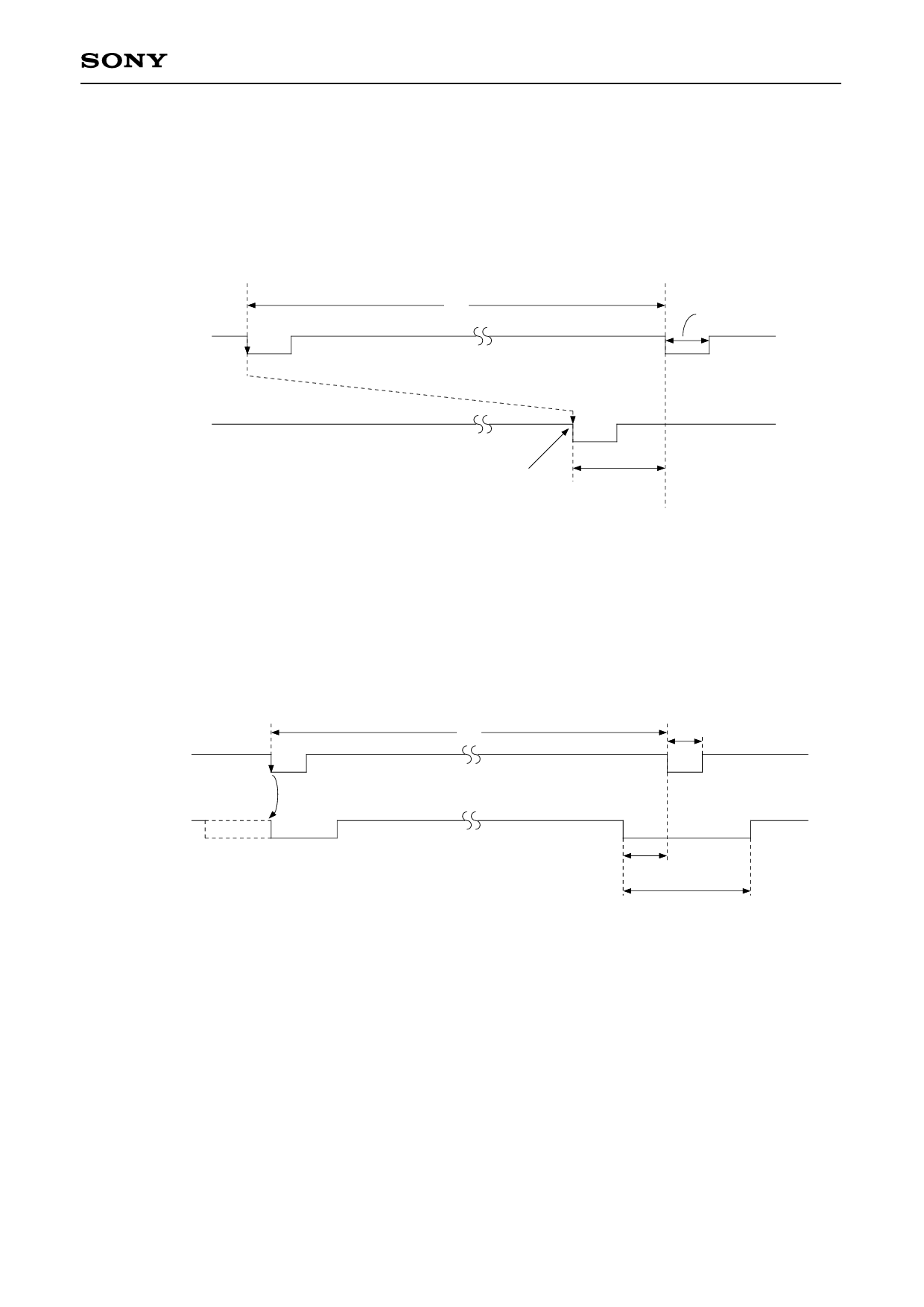
External Synchronization Mode Description
• H Reset
The reset process is started from the first falling edge of the inputted reset pulse. The next reset occurs
only when there is a divergence of at least a clock cycles (0.98 µs) from the edge.
The minimum reset pulse width is 0.98 µs.
The HD output reset position leads the H reset input by 2.45 to 2.94 µs.
H reset input
1H
0.98µs and over
HD output
HD pulse reset at the falling edge of 0.98µs and over
2.45 to 2.94µs
• V Reset
The VD output reset position leads the falling edge of the V reset input by 3.5 to 4.0 H for NTSC/EIA and by
3.0 to 3.5 H for PAL.
The minimum reset pulse width is 32 µs.
V reset input
1V
32µs and over
VD output
3.5 to 4.0H (NTSC/EIA)
3.0 to 3.5H (CCIR)
9H
—11—
Share Link: 