W91030 Ver la hoja de datos (PDF) - Winbond
Número de pieza
componentes Descripción
Fabricante
W91030 Datasheet PDF : 31 Pages
| |||
Preliminary W91030B
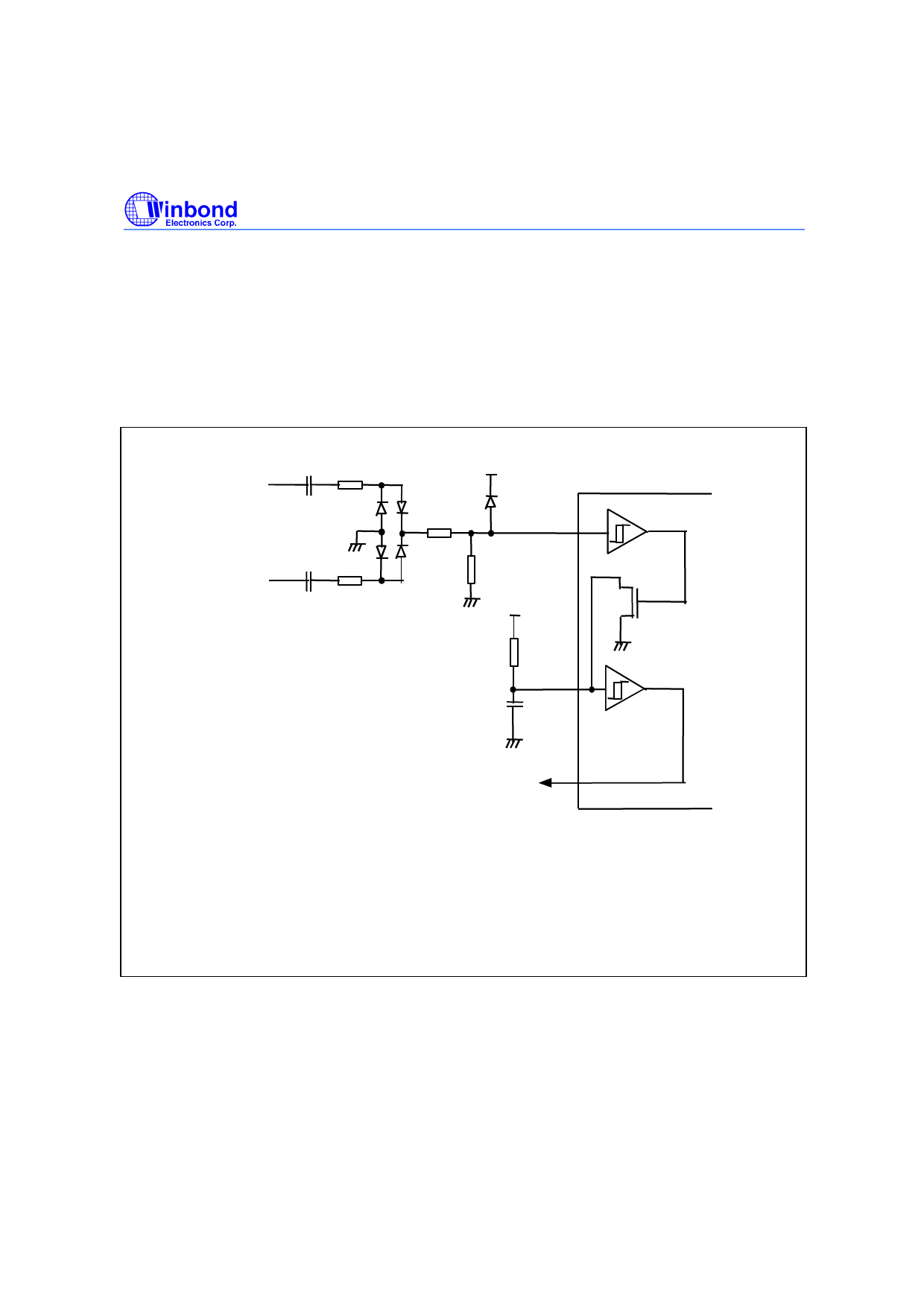
FUNCTIONAL DESCRIPTION
Figure 6 is shown functional blocks of W91030B. The device must operate with a 3.579545 MHz
system clock and consists four major functions and decribed as follows:
Ring Detector
The application circuit in Figure 7-1 illustrates the relationship between the RNGDI, RNGRC and
RNGON signals. The three pin combination is used to detect an increase of the RNGDI voltage from
ground to a level above the Schmitt trigger high going threshold voltage VT+.
C1 = 0.1uF
Tip/A
R1 = 470K
Ring/B
C1 = 0.1 uF
R2 = 470 K
V DD
W91030B
R3 = 200 K
RNGDI
R4 = 300 K
V DD
R5 = 150 K
RNGRC
C3 = 0.22 uF
Allowance minimal ring voltage (peak to peak) is:
Vpp (max ring) = 2 (V T+(max) (R1 + R3 + R4) / R4 + 0.7)
Tolerance to noise between Tip and Ring and Vss is:
Vpeak (max noise) = V T+(min) (R1 + R3 + R4) / R4 + 0.7
Time constant is:
T = R5 C3 ln [VDD / (VDD - V T+ )]
V T+(min) <= V T+ <= V T+(max)
RNGON
R5 from 10K ohm to 500K ohm.
C3 from 47 nF to 0.68 uF.
Figure 7-1. Application Circuit of the Ring Detecter
The RC time constant of the RNGRC pin is used to delay the output pulse of the RNGON pin for a
low going edge on RNGDI. This edge goes from above the VT+ voltage to the Schmitt trigger low
going threshold voltage VT-. The RC time constant must be greater than the maximum period of the
ring signal, to ensure a minimum RNGON low interval and to filter the ring signal to get an envelope
output.
-6-
Share Link: 