STV9380A Ver la hoja de datos (PDF) - STMicroelectronics
Número de pieza
componentes Descripción
Fabricante
STV9380A
STMicroelectronics

STV9380A Datasheet PDF : 10 Pages
| |||
Pin Functions
1 Pin Functions
STV9380A
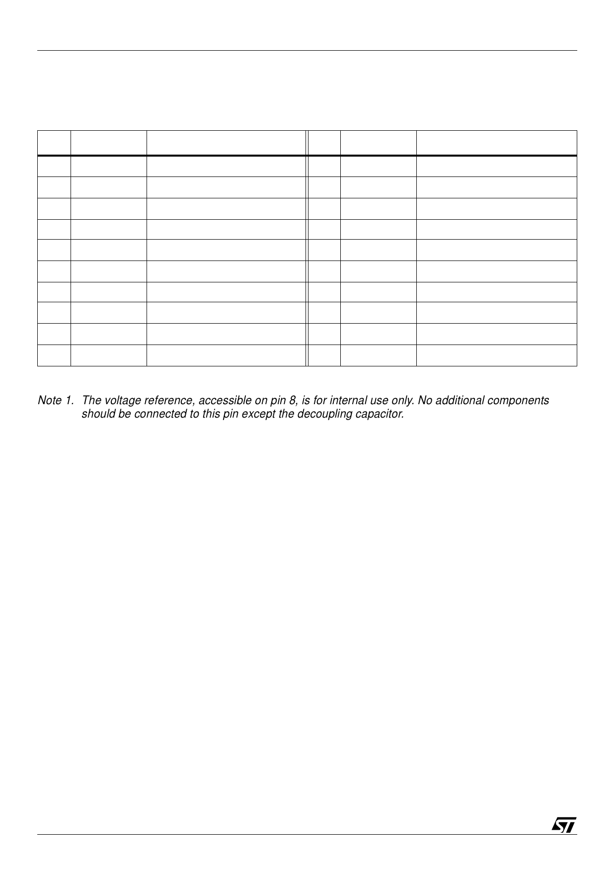
Table 1: STV9380A Pin Descriptions
Pin
Name
Function
1
-VCC
Negative Supply
2
-VCC
Negative Supply
3
-VCC
Negative Supply
4
OUT
PWM Output
5
CFLY+
Flyback Capacitor
6
CFLY-
Flyback Capacitor
7
BOOT
Bootstrap Capacitor
8
VREG
Internal Voltage Regulator
9
FEEDCAP Feed-back Integrating Capacitor
10
FREQ
Frequency Setting Resistor
Pin
Name
Function
11
SGND
Signal Ground
12
IN-
Error Amplifier Inverting Input
13
IN+
Error Amplifier Non-inverting Input
14
EA out
Error Amplifier Output
15
+VCC
Positive Supply
16
+VCCPOW
Positive Power Supply
17
-VccPOW
Negative Power Supply
18
-VCC
Negative Supply
19
-VCC
Negative Supply
20
-VCC
Negative Supply
Note 1. The voltage reference, accessible on pin 8, is for internal use only. No additional components
should be connected to this pin except the decoupling capacitor.
2 Functional Description
The STV9380A is a vertical deflection circuit operating in Class D. Class D is a modulation method
where the output transistors work in switching mode at high frequency. The output signal is restored
by filtering the output square wave with an external LC filter. The major interest of this IC is the
comparatively low power dissipation in regards to traditional amplifiers operating in class AB,
eliminating the need of an heatsink.
Except for the output stage which uses Class D modulation, the circuit operation is similar to the
one of a traditional linear vertical amplifier.
A (sawtooth) reference signal has to be applied to the circuit which can accept a differential or
single ended signal. This sawtooth is amplified and applied as a current to the deflection yoke. This
current is measured by means of a low value resistor. The resulting voltage is used as a feedback
signal to guarantee the conformity of the yoke current with the reference input signal.
The overvoltage necessary for a fast retrace is obtained with a chemical capacitor charged at the
power supply voltage of the circuit. At the flyback moment, this capacitor is connected in series with
the output stage power supply. This method, used for several years with the linear vertical boosters
and called “internal flyback” or “flyback generator”, avoids the need of an additional power supply,
while reducing the flyback duration.
The circuit uses a BCD process that combines Bipolar, CMOS and DMOS devices. The output
stage is composed of low-RON N-channel DMOS transistors.
2/10
Share Link: