STV7617DU Ver la hoja de datos (PDF) - STMicroelectronics
Número de pieza
componentes Descripción
Fabricante
STV7617DU Datasheet PDF : 17 Pages
| |||
STV7617, STV7617D, STV7617U
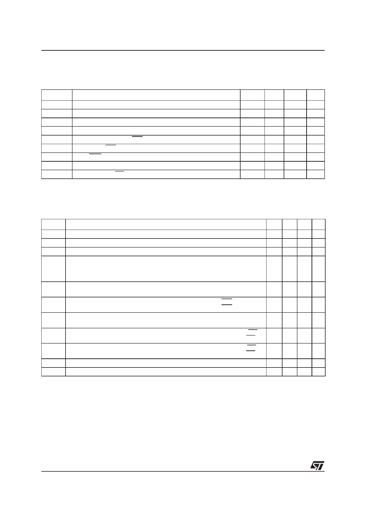
AC TIMING REQUIREMENTS
(VCC = 4.5 V to 5.5 V, Tamb = -20 to +85°C, input signals max leading edge & trailing edge (tR, tF) = 10 ns)
Symbol
tWHCLK
tWLCLK
tSDAT
tHDAT
tDSTB
tSSTB
tSTB
tBLK
tHIZ
Parameter
Duration of clock (CLK) pulse at high level
Duration of clock (CLK) pulse at low level
Set-up Time of data input before clock (low to high) transition
Hold Time of data input after clock (low to high) transition
Minimum Delay to latch STB after clock (low to high) transition
Set-up Time STB before clock (low to high) transition
Latch STB Low Level Pulse Duration
Blanking (BLK) Pulse Duration
High Impedance HIZ Pulse Duration
Min.
40
40
10
20
25
10
20
500
500
Typ.
-
-
-
-
-
-
-
-
-
Max.
-
-
-
-
-
-
-
-
-
Unit
ns
ns
ns
ns
ns
ns
ns
ns
ns
AC TIMING CHARACTERISTICS
(VCC = 5 V, VPP = 90 V, VSSP = 0 V, VSSLOG = 0 V, VSSSUB = 0 V, Tamb = 25°C, VILMax. = 0.2 Vcc,
VIHMin. = 0.8 VCC, VOH = 4.0 V, VOL = 0.4 V, unless otherwise specified)
Symbol
Parameter
Min. Typ. Max. Unit
tCLK
tRDAT
tFDAT
tPHL1
tPLH1
Data Clock Period
Logical Data Output Rise Time
Logical Data Output Fall Time
Delay of logic data output (high to low transition) after clock (CLK) transition
(CL=10pF)
Delay of logic data output (low to high transition) after clock (CLK) transition
(CL=10 pF)
125 - - ns
- 12 20 ns
- 10 20 ns
- 37 50 ns
- 42 60 ns
tPHL2 Delay of power output change (high to low transition) after clock (CLK) transition
-
tPLH2 Delay of power output change (low to high transition) after clock (CLK) transition
-
tPHL3 Delay of power output change (high to low transition) after Latch (STB) transition
-
tPLH3 Delay of power output change (low to high transition) after Latch (STB) transition
-
tPHL4 Delay of power output change (high to low transition) to blank (BLK) transition
-
tPLH4 Delay of power output change (low to high transition) to blank (BLK) transition
-
tPHZ5 Delay of power output change (high to Hi-Z transition) after high impedance (HIZ)(9) -
tPLZ5 Delay of power output change (low to Hi-Z transition) after high impedance (HIZ)(9) -
tPZH5 Delay of power output change (Hi-Z to high transition) after high impedance (HIZ) (9) -
tPZL5 Delay of power output change (Hi-Z to low transition) after high impedance (HIZ) (9) -
tROUT Power Output Rise Time (10)
-
tFOUT Power Output Fall Time (10)
-
110 180 ns
115 180 ns
80 165 ns
95 165 ns
75 160 ns
75 160 ns
40 160 ns
80 160 ns
75 160 ns
40 160 ns
175 350 ns
35 150 ns
Note 9 See test diagram page 12.
Note 10 One output among 64, loading capacitor COUT = 200pF, other outputs at low level.
10/17
3
Share Link: 