STV0056 Ver la hoja de datos (PDF) - STMicroelectronics
Número de pieza
componentes Descripción
Fabricante
STV0056 Datasheet PDF : 37 Pages
| |||
STV0042/STV0056 APPLICATION NOTE
3 - APPLICATION NOTES (continued)
f) Dimensioning the External Components
(DET, AMPLOCK, AGC, CPUMP Pins)
Example : Left channel (see Figure 10).
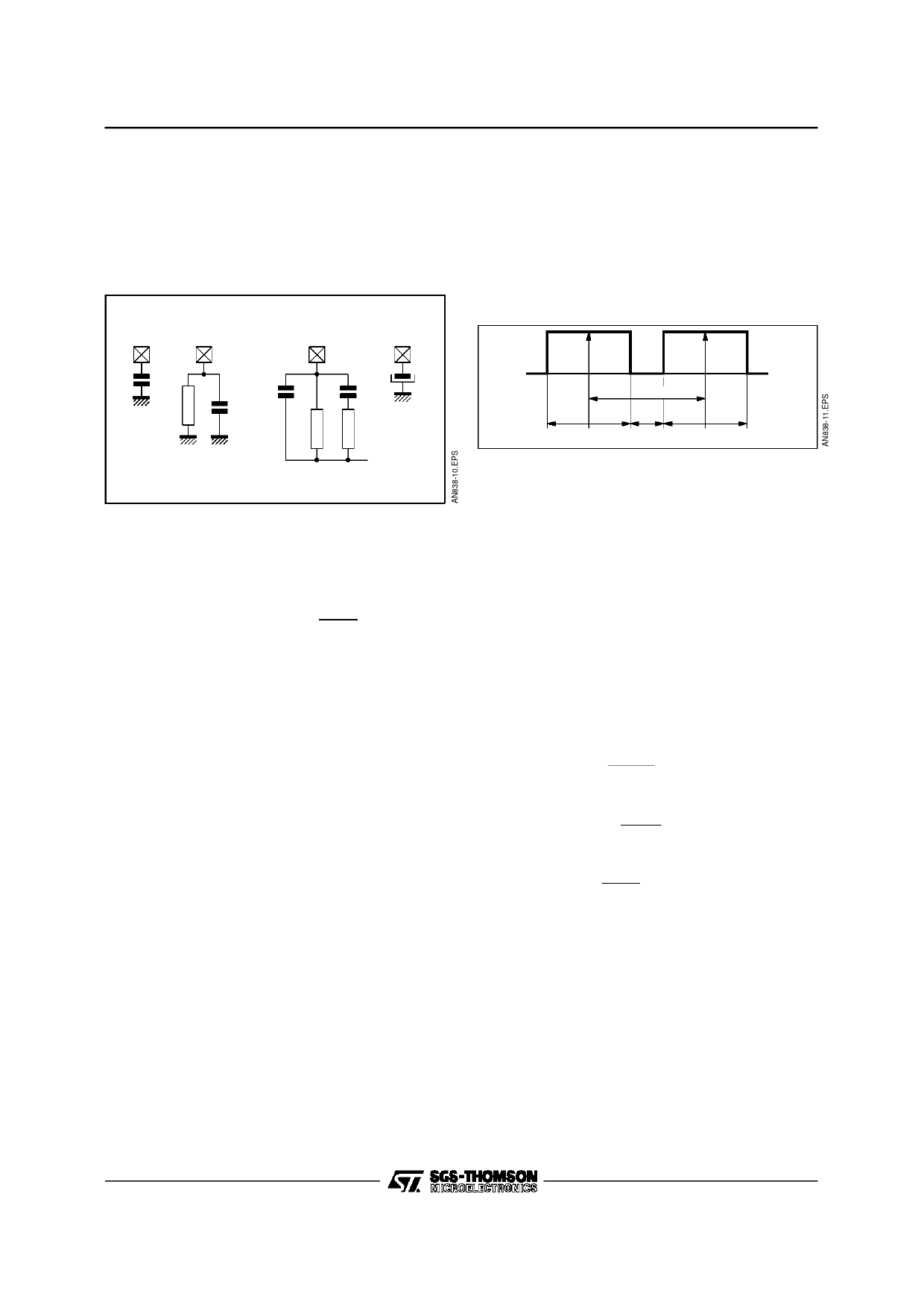
Figure 10 : Left Channel, FM Demodulator
External Components
AGC AMPLOCK
DET
CPUMP
The most severe case is : ”narrow band stereo pair”
when simultaneously are required a good quality
sound and a precise control of the capture range
(due to the low frequency spacing : 180kHz (80kHz
dynamically)).
Figure 11 : Stereo Pair, Frequency Spacing and
Coverage
C43
R36
C38
C49
R33
C41
C37
R32
VREF
- AMPLOCK, AGC Pins :
Due to the AGC loop, the amplitude As of the
wanted subcarrier at the phase detector input is
inversely proportionnal to the external resistor
connected to AMPPLOCK.
(As)PP
≈
π
⋅
DETH
⋅
11kΩ
R36
In order to maintain the phase detector in a linear
operation (even in case of a high number of
subcarrier : 10 subcarriers), we recommand (As)
not to exeed 0.25VPP.
For R36 = 560kΩ, AsPP ≈ 0.19 VPP.
The C49 capacitor associated with R36 realizes a
filter which rejects all the AC components. For a
good operation, the roll-off frequency of this filter
is lower than the audio spectrum for C49 = 100nF,
fC ≈ 2.8MHz.
The value of the AGC capacitor C43 is not very
critical, 100nF has been selected for component
standardization. However it is recommanded to
have C43 < 1µF for a good stability of the loop.
- CPUMP Pin :
Choosing the CPUMP capacitor value results
from a compromisze. The smaller is CPUMP the
shorter is the duration of the frequency synthesis,
but a too small value of CPUMP induces a too fast
response of the DC compensating loop (risk of
distorsion in the low frequency audio signals).
C41 = 10µF is a good compromise.
- DET Pins :
following is a simplified method to calculate the
components.
180k
50k 50k 80k 50k 50k
FSB L
FSB R
Theoretical request : ωL > 50kHz, ωC < 80kHz.
Actually a more severe compromise is required.
- ωL > 70kHz. A first margin is required to compen-
sate the phase lag which appears in case of high
frequency slew rates (case of audio sibilance). In
practice, a further margin is given to compensate
the dispersion of the phase detector gain, even-
tually :
90kHz ≤ ωL typ. ≤ 100kHz
- ωC will be choosen as low as possible to also
compensate potential level imbalance between
left and right subcarriers (2 to 3dB max. could be
measured on some broadcasted channels).
The STV42/56 circuits have been optimized to get
a 1VPP at the DET Pin (full deviation).
Refering to realation (2) :
K
⋅
KO
=
100kHz
1VPP PP
=
100kHz/V
choosing ωL = 100kHz in (1) :
KD
=
K
ωL
⋅ KO
≈
1V/rd
using relation (0) :
R33
=
KD
DETH
⋅
R36
≈
180kΩ,
DETH = 3.1V, R36 = 560kΩ
To calculate the other components C37, R32, would
lead to complex mathematics. A first estimate can
be done using the relations given in Annex 1.
Some experiments and calculations have given
R32 = 82kΩ and C37 = 22pF, corresponding cap-
ture range is about 52kHz.
An additionnal capacitor C38 is recommanded to
give a further reduction to the capture range
(C38 ≈ 15 to 22pF).
11/37
Share Link: 