STK672-600 Ver la hoja de datos (PDF) - SANYO -> Panasonic
Número de pieza
componentes Descripción
Fabricante
STK672-600 Datasheet PDF : 19 Pages
| |||
STK672-600
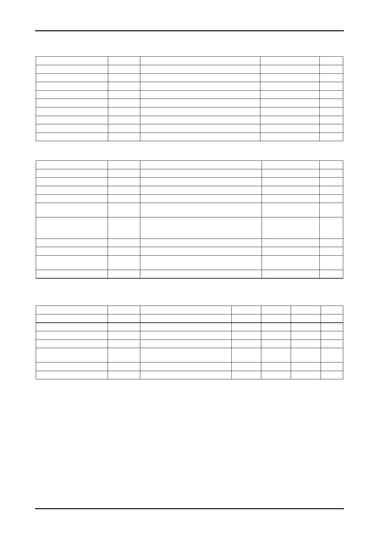
Specifications
Absolute Maximum Ratings at Tc = 25°C
Parameter
Maximum supply voltage 1
Maximum supply voltage 2
Input voltage
Output current
Allowable power dissipation 1
Allowable power dissipation 2
Operating substrate temperature
Junction temperature
Storage temperature
Symbol
VCC max
VDD max
VIN max
IOH max
PdMF max
PdPK max
Tc max
Tj max
Tstg
Conditions
No signal
No signal
Logic input pins
VDD=5V, CLOCK≥200Hz
With an arbitrarily large heat sink. Per MOSFET
No heat sink
Ratings
unit
52
V
-0.3 to +7.0
V
-0.3 to +7.0
V
2.65
A
7.8
W
3.1
W
105
°C
150
°C
-40 to +125
°C
Allowable Operating Ranges at Ta = 25°C
Parameter
Symbol
Conditions
Ratings
unit
Operating supply voltage 1
VCC
With signals applied
10 to 42
V
Operating supply voltage 2
VDD
With signals applied
5±5%
V
Input high voltage
Input low voltage
VIH
Pins 10, 12, 13, 14, 15, 17
VIL
Pins 10, 12, 13, 14, 15, 17
2.5 to VDD
V
0 to 0.6
V
Output current 1
IOH1
Tc=105°C, CLOCK≥200Hz,
Continuous operation, duty=100%
2.0
A
Output current 2
IOH2
Tc=80°C, CLOCK≥200Hz,
Continuous operation, duty=100%,
2.2
A
CLOCK frequency
See the motor current (IOH) derating curve
fCL
Minimum pulse width: at least 10μs
0 to 50
kHz
Phase driver withstand voltage
VDSS
ID=1mA (Tc=25°C)
100min
V
Recommended operating
substrate temperature
Tc
No condensation
0 to 105
°C
Recommended Vref range
Vref
Tc=105°C
0.14 to 1.38
V
Refer to the graph for each conduction-period tolerance range for the output current and brake current.
Electrical Characteristics at Tc = 25°C, VCC = 24V, VDD = 5.0V
Parameter
Symbol
Conditions
min
typ
VDD supply current
ICCO
Pin 9 current CLOCK=GND
5.0
Output average current
Ioave
R/L=1Ω/0.62mH in each phase
0.362
0.402
FET diode forward voltage
Vdf
If=1A (RL=23Ω)
1.0
Output saturation voltage
Vsat
RL=23Ω
0.42
Input leak current
IIL
Pins 10, 12, 13, 14, 15, 17
=GND and 5V
Vref input bias current
IIB
Pin 19 =1.0V
204
PWM frequency
fc
35
45
*Ioave values are for when the lead frame of the product is soldered to the mounting substrate.
Notes: A fixed-voltage power supply must be used.
max
unit
9
mA
0.442
A
1.6
V
0.61
V
±10
μA
216
μA
56 kHz
No. A0755-2/19
Share Link: 