STK621-017 Ver la hoja de datos (PDF) - SANYO -> Panasonic
Número de pieza
componentes Descripción
Fabricante
STK621-017 Datasheet PDF : 8 Pages
| |||
STK621-017
TENTATIVE
01.Nov.2002
*Notes
Lower side →It outputs FAULT signal with gate signal OFF.
However, it different from the protection operation of upper side, it is automatically reset
about 9 ms later and becomes an operation beginning condition when recovering to the normal
voltage. (The protection operation doesn't latch by the input signal.)
3.When assembling the hybrid IC on the heat sink, tightening torque range is 0.8N・m to 1.0N・m.
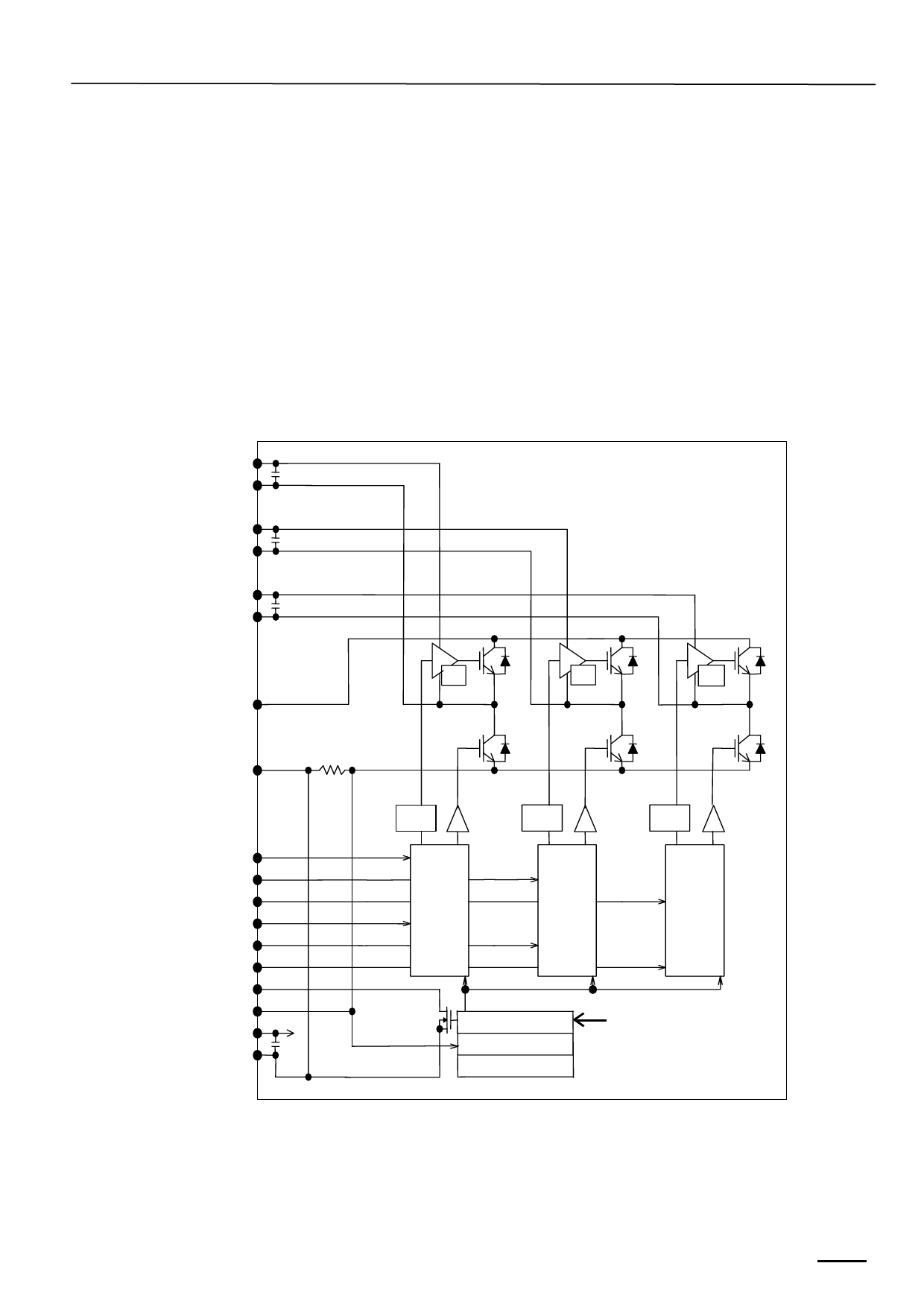
Circuit Block Diagram
VB1( 8)
CB
U( 9)
VB2( 5)
CB
V( 6)
VB3( 2)
CB
W( 3)
+ (11)
U .V .
U .V .
U .V .
− (13)
H IN 1 (1 4 )
HIN2(15)
HIN3(16)
LIN1(17)
LIN2(18)
LIN3(19)
Fault(20)
Iso( 21)
V D D (2 2 )
Vss(23)
Shunt Resistor
Level
Shifter
Logic
Level
Shifter
Logic
Level
Shifter
Logic
Latch
Over-Current
VDD-Under Voltage
Latch Time About 9ms
( Automatic Reset )
────────────────────────────────────────────
SANYO Electric Co.,Ltd. Semiconductor Company
No.3/8
Share Link: 