STK4040XI Ver la hoja de datos (PDF) - SANYO -> Panasonic
Número de pieza
componentes Descripción
Fabricante
STK4040XI Datasheet PDF : 5 Pages
| |||
STK4040XI
Description of External Parts
R1, C1
C2
R2
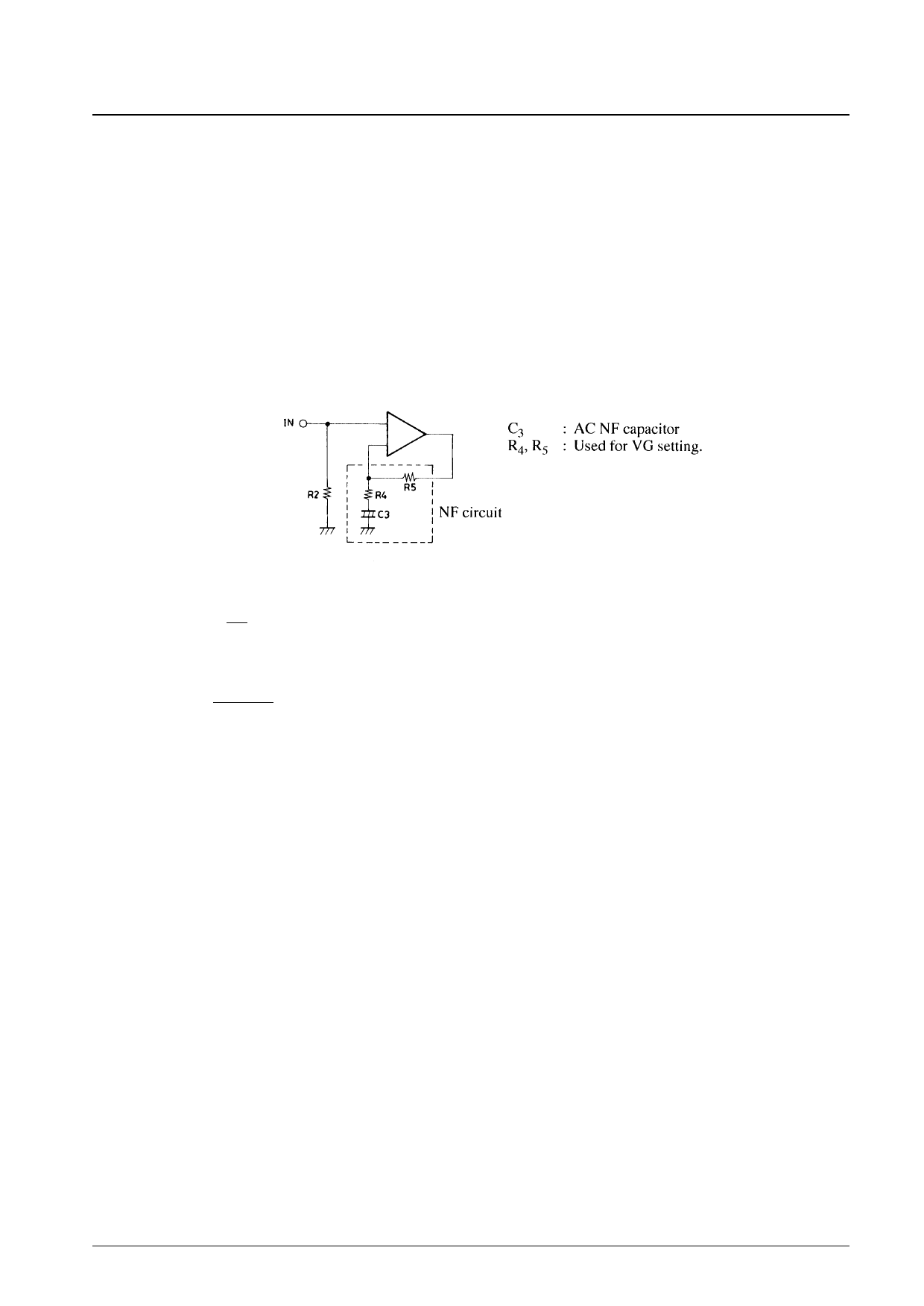
R4, R5
C3 (R2)
: Input filter circuit
• Reduces high-frequency noise.
: Input coupling capacitor
• DC current suppression. A reduction in reactance is effective because of increases in capacitor reactance
at low frequencies and 1/f noise dependence on signal source resistance which result in output noise
worsening.
: Input bias resistor
• Biases the input pin to zero.
• Effects VN stability (refer to NF circuit).
• Due to differential input, input resistance is more or less determined by this resistance value.
: NFB circuit (AC NF circuit). Use of resistor with 1% error is suggested.
R3
R6, R7
R7, C4
C6, C9
C8
C5
R8, C10
R9, C13
C11, C12
R10
• VG settings are obtained using R4 and R5 according to the following equation:
log20·
R5
R4
40 dB is recommended.
• Low-frequency cutoff frequency settings are obtained using R4 and C3 according to the following
equation:
1
fL = 2π·R4·C3 [Hz]
When changing the VG setting, you should change R4 which requires a recheck of the low cutoff frequency
setting. When the VG setting is changed using R5, the setting should ensure R2 equals R5 so that VN
balance stability is maintained. If the resistor value is increased more than the existing value, VN balance
may be disturbed and result in deterioration of VN temperature characteristics.
: Differential constant-current bias resistor
: For oscillation suppression and phase compensation applications
(For use with differential stage applications)
: For oscillation suppression and phase compensation applications
(A Mylar capacitor is recommended for C4 for use with output stage applications)
: For oscillation suppression and phase compensation applications
Power stage (Must be connected near the pin) C6: Positive (+) power C9: Negative (–) power
: For oscillation suppression and phase compensation applications
(Oscillation suppression before power step clip)
: For oscillation suppression and distortion improvement applications
: Ripple filter circuit on positive (+) side.
: Ripple filter circuit on negative (–) side.
: For oscillation suppression applications
• Used for reducing power supply impedance to stable IC operation and should be connected near the IC
pin. We recommend that you use an electrolytic capacitor.
: Output resistor
Increases load shorting endurance capacity during times of high output.
No. 4621-4/5
Share Link: 