STE2001DIE2 Ver la hoja de datos (PDF) - STMicroelectronics
Número de pieza
componentes Descripción
Fabricante
STE2001DIE2 Datasheet PDF : 36 Pages
| |||
STE2001
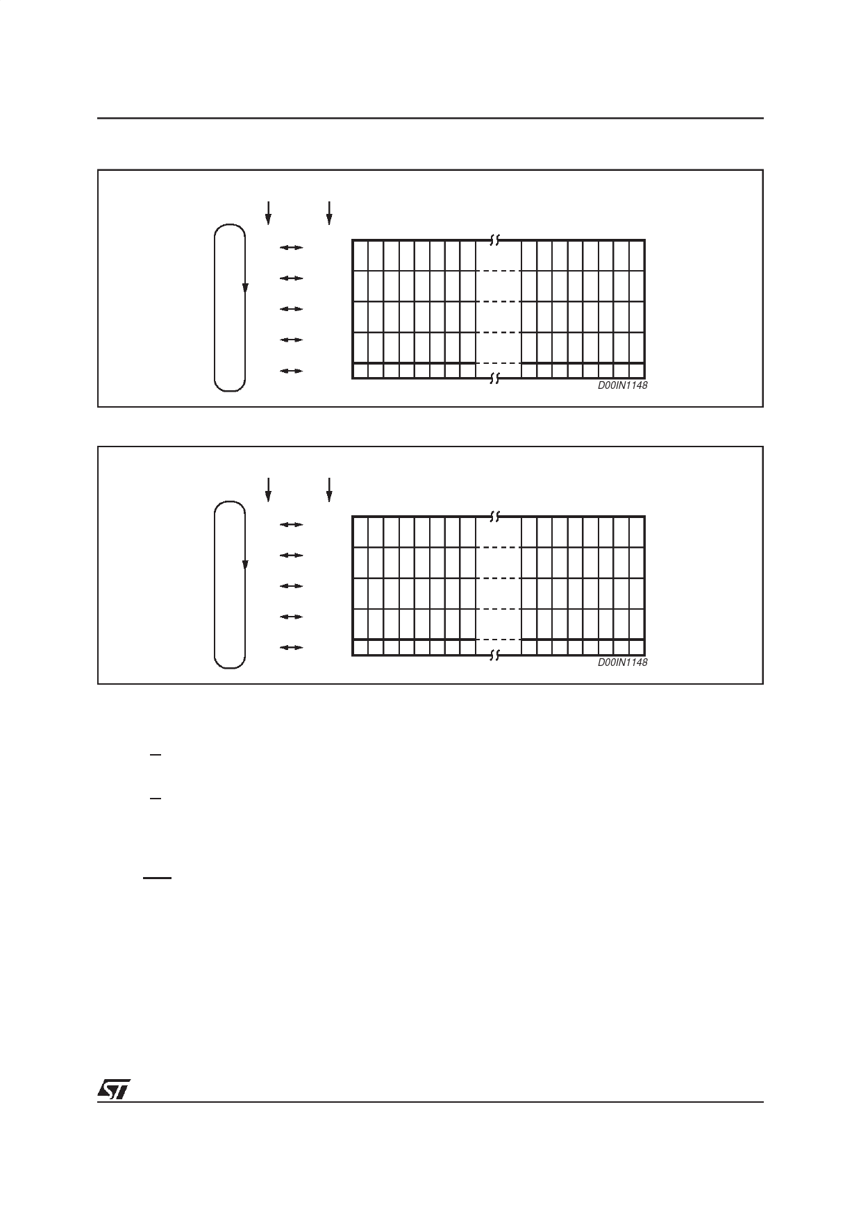
Figure 11. Output drivers rows and logical memory rows correspondence with MY = 0
ROW DRIVER MUX 33 PHYSICAL MEMORY ROW
01234567
120 121 122 123 124 125 126 127
R16
Row 0
to
to
R23
Row 7
BANK 4
R24
Row 8
to
to
R31
Row15
BANK 5
R48
Row 16
to
to
R55
Row 23
BANK 6
R56
Row 24
to
to
R63
Row 31
BANK 7
R64
Row 32
BANK 8
D00IN1148
Figure 12. Output drivers rows and logical memory rows correspondence with MY = 1
ROW DRIVER MUX 33 PHYSICAL MEMORY ROW
01234567
120 121 122 123 124 125 126 127
R16
Row 0
to
to
R23
Row 7
BANK 4
R24
Row 8
to
to
R31
Row15
BANK 5
R48
Row 16
to
to
R55
Row 23
BANK 6
R56
Row 24
to
to
R63
Row 31
BANK 7
R64
Row 32
BANK 8
D00IN1148
Instruction Set
Two different instructions formats are provided:
- With D/C set to LOW
commands are sent to the Control circuitry.
- With D/C set to HIGH
the Data RAM is addressed Instructions have the syntax summarized in Table.1.
Reset (RES)
At power-on, all internal registers and RAM content are not defined. A Reset pulse must be applied on RES pad
(active low) to initialize the internal registers content (see Tables 3,4,5,&6). Every on-going communication with
the host controller is interrupted. The IC after the reset pulse is programmed in Power Down mode.
The Default configurations is:
- Horizontal addressing (V = 0)
- Normal instruction set (H = 0)
- Normal display (MX = MY = TRS =BRS = 0)
- MUX 65 mode (MUX = 0)
11/36
Share Link: 