ST8024CD Ver la hoja de datos (PDF) - STMicroelectronics
Número de pieza
componentes Descripción
Fabricante
ST8024CD Datasheet PDF : 23 Pages
| |||
ST8024
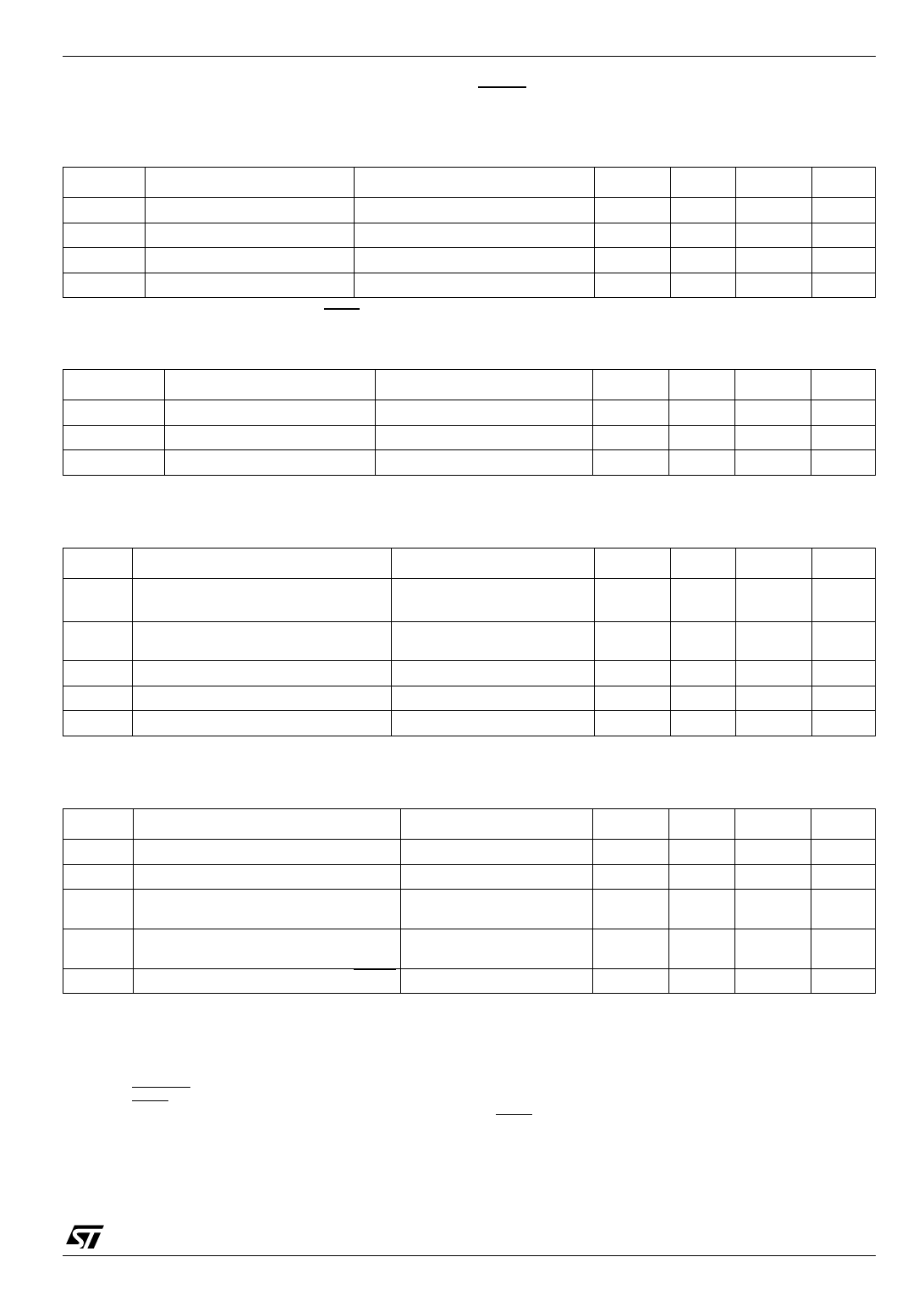
Table 16: Card Presence Inputs (PINS PRES AND PRES)
(VDD = 3.3V, VDDP = 5V, fXTAL = 10MHz, unless otherwise noted. Typical values are to Ta = 25°C) (Note
6)
Symbol
VIL
VIH
|ILIH|
|ILIL|
Parameter
Test Conditions
Input Voltage LOW
Input Voltage HIGH
Input Leakage Current HIGH VIH = VDD
Input Leakage Current LOW VIL = 0
Min.
-0.3
0.7 VDD
Typ.
Max.
0.3 VDD
VDD+0.3
5
5
Unit
V
V
µA
µA
Table 17: Interrupt Output (PIN OFF NMOS Drain With Integrated 20 kΩ PULL-UP Resistor To
VDD); (VDD = 3.3V, VDDP = 5V, fXTAL = 10MHz, unless otherwise noted. Typical values are to Ta = 25°C)
Symbol
VOL
VOH
RPU
Parameter
Low Level Output Voltage
High Level Output Voltage
Integrated pull-up resistor
Test Conditions
IOL = 2 mA
IOH = -15 µA
20kΩ Pull-up resistor to VDD
Min.
0
0.75 VDD
16
Typ.
20
Max.
0.3
24
Unit
V
V
kΩ
Table 18: Protection And Limitation (VDD = 3.3V, VDDP = 5V, fXTAL = 10MHz, unless otherwise noted.
Typical values are to Ta = 25°C)
Symbol
Parameter
|ICC(SD)| Shutdown and limitation current pin
VCC
II/O(lim) limitation current pins I/O, AUX1 and
AUX2
ICLK(lim) limitation current pin CLK
IRST(lim) limitation current pin RST
TSD Shut down temperature
Test Conditions
Min.
90
-15
-70
-20
Typ.
150
Max. Unit
120
mA
15
mA
70
mA
20
mA
°C
Table 19: Timing (VDD = 3.3V, VDDP = 5V, fXTAL = 10MHz, unless otherwise noted. Typical values
are to Ta = 25°C)
Symbol
Parameter
Test Conditions
tACT Activation time
(See Fig. 5)
tDE Deactivation time
(See Fig. 7)
t3 Start of the window for sending CLK (See Fig. 6)
to the card
t5 End of the window for sending CLK to (See Fig. 6)
card
tdebounce Debounce time pins PRES and PRES (See Fig. 8)
Min.
50
50
50
140
5
Typ.
80
8
Max. Unit
220
µs
100
µs
130
µs
220
µs
11
ms
Note 1: All parameters remain within limits but are tested only statistically for the temperature range. When a parameter is specified as a
function of VDD or VCC it means their actual value at the moment of measurement.
Note 2: To meet these specifications, pin VCC should be decoupled to CGND using two ceramic multilayer capacitors of low ESR both with
values of 100 nF and 100 nF (see Fig.10).
Note 3: Permitted capacitor values are 100 + 100 nF, or 220 nF.
Note 4: Transition time and duty factor definitions are shown in Fig.3; δ = t1/(t1+ t2).
Note 5: Pin CMDVCC is active LOW; pin RSTIN is active HIGH; for CLKDIV1 and CLKDIV2 functions see Table 20.
Note 6: Pin PRES is active LOW; pin PRES is active HIGH see Figs. 8 and 9; PRES has an integrated 1.25 µA current source to GND
(PRES to VDD); the card is considered present if at least one of the inputs PRES or PRES is active.
9/23
Share Link: 