ST8024CD Ver la hoja de datos (PDF) - STMicroelectronics
Número de pieza
componentes Descripción
Fabricante
ST8024CD Datasheet PDF : 23 Pages
| |||
ST8024
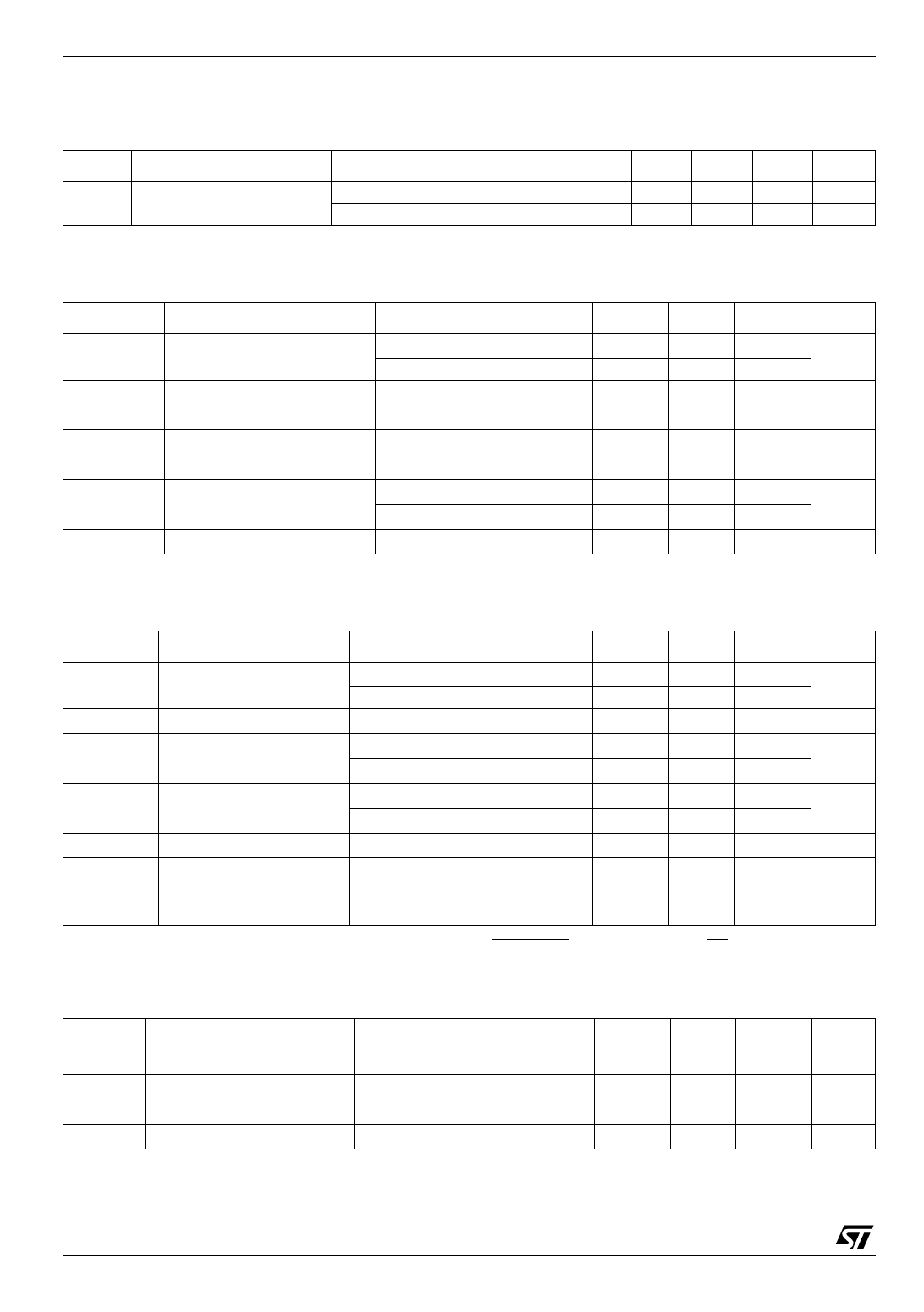
Table 12: Internal Oscillator (VDD = 3.3V, VDDP = 5V, fXTAL = 10MHz, unless otherwise noted.
Typical values are to Ta = 25°C)
Symbol
Parameter
fOSC(INT) Frequency of internal
oscillator
Test Conditions
Inactive mode
Active mode
Min.
55
2.2
Typ.
140
2.7
Max.
200
3.2
Unit
kHz
MHz
Table 13: Reset Output To Card Reader (PIN RST) (VDD = 3.3V, VDDP = 5V, fXTAL = 10MHz, unless
otherwise noted. Typical values are to Ta = 25°C)
Symbol
VO(inactive)
Parameter
Output Voltage in Inactive
Mode
IO(inactive) Output Current
tD(RSTIN-RST) RSTN to RST Delay
VOL
Low Level Output Voltage
VOH
High Level Output Voltage
tR, tF
Rise and fall time
Test Conditions
IO(inactive) = 1 mA
No Load
Inactive mode; pin grounded
RST Enable
IOL = 200 µA
IOL = 20 mA (current limit)
IOH = -200 µA
IOH = -20 mA (current limit)
CL = 100 pF; VCC = 5 or 3 V
Min.
0
0
0
0
VCC-0.4
0.9VCC
0
Typ.
Max.
0.3
0.1
-1
2
0.2
VCC
VCC
0.4
0.1
Unit
V
mA
µs
V
V
µs
Table 14: Clock Output To Card Reader (PIN CLK) (VDD = 3.3V, VDDP = 5V, fXTAL = 10MHz, unless
otherwise noted. Typical values are to Ta = 25°C)
Symbol
Parameter
Test Conditions
VO(inactive)
IO(inactive)
VOL
VOH
tR, tF
δ
SR
Output Voltage in Inactive
Mode
Output Current
IO(inactive) = 1 mA
No Load
CLK Inactive mode; pin grounded
Low Level Output Voltage
High Level Output Voltage
Rise and fall time
Duty factor (except for
fXTALS)
Slew Rate
IOL = 200 µA
IOL = 70 mA (current limit)
IOH = -200 µA
IOH = -70 mA (current limit)
CL = 30 pF (Note 4)
CL = 30 pF (Note 4)
Slew up or down; CL = 30 pF
Min.
0
0
0
0
VCC-0.4
0.9VCC
0
45
0.2
Typ.
Max.
0.3
0.1
-1
0.3
VCC
VCC
0.4
16
55
Unit
V
mA
V
V
ns
%
V/ns
Table 15: Control Inputs (PINS CLKDIV1, CLKDIV2, CMDVCC, RSTIN AND 5V/3V
(VDD = 3.3V, VDDP = 5V, fXTAL = 10MHz, unless otherwise noted. Typical values are to Ta = 25°C) (Note
5)
Symbol
Parameter
Test Conditions
VIL
VIH
|ILIH|
|ILIL|
Input Voltage LOW
Input Voltage HIGH
Input Leakage Current HIGH VIH = VDD
Input Leakage Current LOW VIL = 0
Min.
-0.3
0.7VDD
Typ.
Max.
0.3VDD
VDD
1
1
Unit
V
V
µA
µA
8/23
Share Link: 