ST7093 Ver la hoja de datos (PDF) - Sitronix Technology Co., Ltd.
Número de pieza
componentes Descripción
Fabricante
ST7093 Datasheet PDF : 43 Pages
| |||
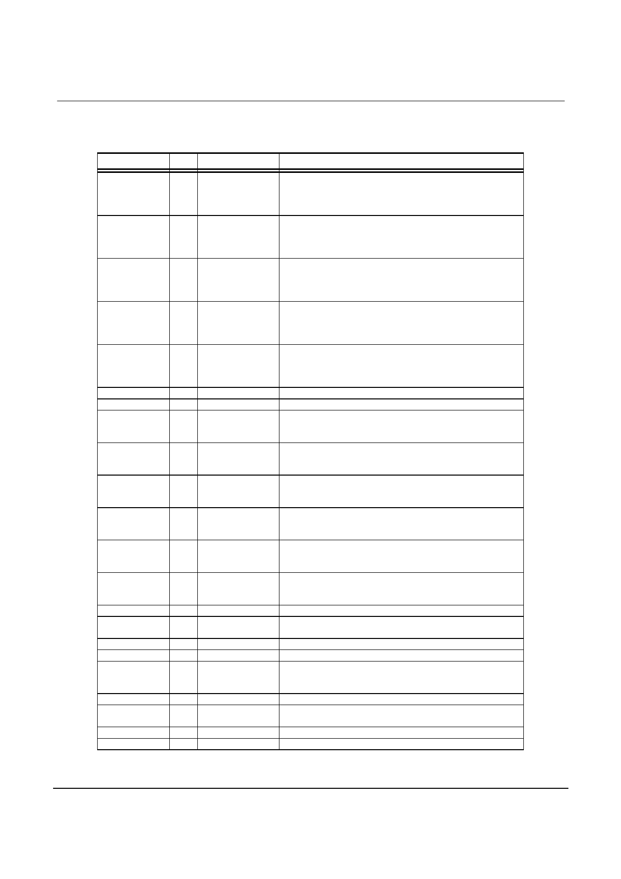
ST7093
PIN DESCRIPTION
NAME I/O Interfaced
FUNCTION
Select registers.
RS
I
MPU
0: Instruction register (for write)
address counter (for read)
1: Data register (for write and read)
Select read or write.
RW_WR
I
MPU
In 68 mode
0: Write
In 80 mode
0: Write
1: Read
1: Not active
Starts data read/write.
E_RD
I
MPU
In 68 mode
0: Not active
In 80 mode
0: Read
1: Enable
1: Not active
Four high order bi-directional tristate data bus
DB4 to DB7 I/O
MPU
pins. Used for data transfer and receive
between the MPU and the ST7093. In serial interface mode
DB7 is SI (input data), DB6 is SCL (serial clock).
Four low order bi-directional tristate data bus
DB0 to DB3 I/O
MPU
pins. Used for data transfer and receive
between the MPU and the ST7093.
These pins are not used during 4-bit operation. (Fixed high)
CSB
I
MPU
Chip select signal. Active low.
RESETB
I
MPU
Reset signal. Active low.
External clock input pin. it must be fixed to “Vss” , when the
CK
I
MPU
internal oscillator circuit is used. In case of the external clock
mode, CK is used as the clock and OS bit should be turn off.
Interface selection
MI
I
MPU
0: 80 mode interface
1: 68 mode interface
DIRS
I
MPU
SEG direction selection
0: SEG1 Æ SEG80
1: SEG80 Æ SEG1
Interface selection valid when PS=1
IF
I
MPU
0: 4 bit bus mode
1: 8 bit bus mode
Interface selection
PS
I
MPU
0: serial mode
1: 4bit/ 8bit bus mode
COM1 to
COM24
O
LCD
Common signals. COMI1 and COMI2 are the same signal
COMI1,COMI2
SEG1 to SEG80 O
LCD
Segment signals
CAP1+, CAP1-
CAP2+, CAP2-
O
Capacitor connection pins for voltage booster
Vout
I/O
Voltage booster output pin
VR
I
Voltage adjust pin between V0 and VSS
Reference voltage selection pin
REF
I
MPU
0: internal regulator is selected
1: external reference voltage input to Vext
Vext
I/O
External reference voltage input
V0 to V4
-
Power supply
Power supply for LCD drive
V0 - Vss = 7 V (Max)
VDD , GND
-
Power supply VDD : 2.4V to 3.6V, GND: 0V
Test 0 to Test3 I
Test pin. open
Note: 1. V0>=V1>=V2>=V3>=V4>=VSS must be maintained
Ver 2.1
6/43
2003/09/23
Share Link: 