ST7032 Ver la hoja de datos (PDF) - Sitronix Technology Co., Ltd.
Número de pieza
componentes Descripción
Fabricante
ST7032 Datasheet PDF : 63 Pages
| |||
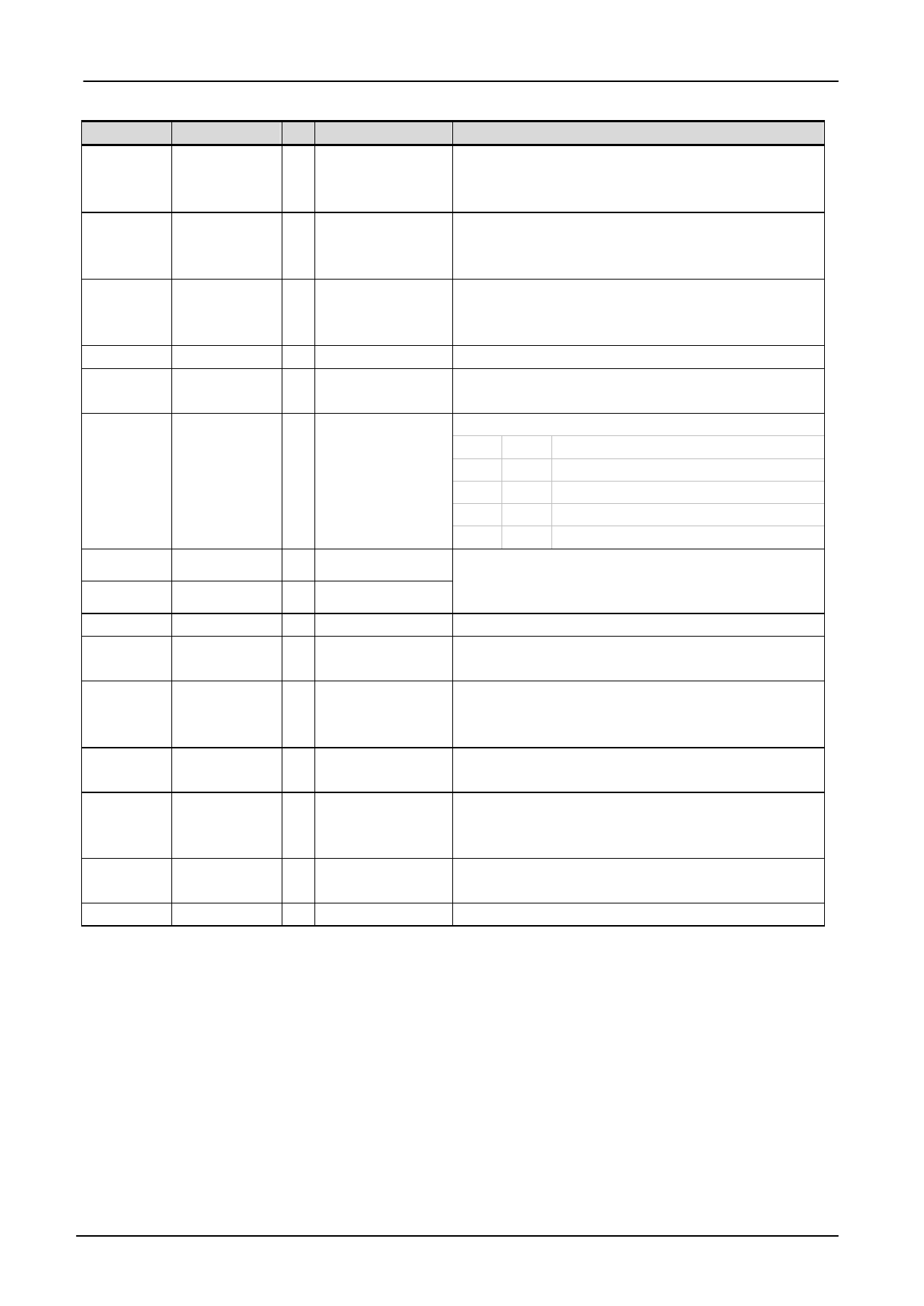
ST7032
Name
SHLC
SHLS
COM1 to
COM16
COMI
SEG1 to
SEG80
OPF1
OPF2
CAP1P
CAP1N
VIN
VOUT
V0 to V4
VDD
VSS
CLS
OSC1
OSC2
TEST1,2
Number
1
1
16
2
I/O Interfaced with
Function
Common signals direction select:
I
ITO option
0:Com1~16←Row address 15~0(Invert)
1:Com1~16←Row address 0~15(Normal)
Segment signals direction select:
I
ITO option
0:Seg1~80←Column address 79~0(Invert)
1:Seg1~80←Column address 0~79(Normal)
Common signals that are not used are changed to
O
LCD
non-selection waveform. COM9 to COM16
are non-selection waveforms at 1/8 or 1/9 duty factor
O
LCD
ICON common signals
80
O
LCD
Segment signals
The built-in voltage follower circuit selection
OPF1 OPF2
Bias select
0
0 Built-in voltage follower(only use at EXT=0)
2
I
ITO option
0
1 Built-in bias resistor(3.3KΩ) ±30%
1
0 Built-in bias resistor(9.6KΩ) ±30%
1
1 External bias resistor select
1
-
Power supply For voltage booster circuit(VDD-VSS)
External capacitor about 0.1u~4.7uf
1
-
Power supply
1
-
Power supply Input the voltage to booster
DC/DC voltage converter. Connect a capacitor between this
1
-
Power supply
terminal and VIN when the built-in booster is used.
Power supply for LCD drive
5
-
Power supply V0-Vss = 7V (Max)
Built-in/external Voltage follower circuit
VDD : 2.7V to 5.5V, VSS: 0V
2
-
Power supply
Internal/External oscillation select
I
ITO option
0:external clock
1:internal oscillation
When the pin input is an external clock, it must be input to
2
I/O
Oscillation
OSC1.
2
I/O
Test pin
TEST1,2 must connect to VDD.
V1.4
8/61
2008/08/18
Share Link: 