ST5451 Ver la hoja de datos (PDF) - STMicroelectronics
Número de pieza
componentes Descripción
Fabricante
ST5451 Datasheet PDF : 34 Pages
| |||

2 - 2 - FIFO Structure
2 - 2 - 1 - Receive FIFO Structure
In receive direction, a 64 byte FIFO memory is
used. It is divided in 8 blocks of 8 bytes automat-
ically chained.
In case of a frame length of 64 bytes or less, the
whole frame can be stored in the FIFO. After the
first 32 bytes have been received µP is inter-
rupted and may read the available data.
In case of frames longer than 64 bytes, the µP is
interrupted to read out the FIFO by 32 byte block.
In case of several short frames, up to eight may be
stored inside the FIFO. After an interrupt, one frame
is available for the µP. The eventual other seven
frames are queuedand transferred one by one.
2 - 2 - 2 - Transmit FIFO Structure
In transmit direction, a 64 byte FIFO memory is
ST5451
used, structured in 2 blocks of 32 bytes. ST5451
is requested to transmit after 32 bytes have been
written into the FIFO.
If a transmission request does not include a mes-
sage end, the HDLC controller will request the
next data block by an interrupt.
2 - 3 - Microprocessor Interface
Three types of microprocessor interfaces are
available (MULT and I/M control pins set the de-
sired interface).
- Motorola non multiplexed families.
- Motorola multiplexed family (6805 type)
- Intel family.
You can connect ST5451 to a Direct Memory Ac-
cess Controller as MC68440 or MC6450 (dual or
quad channels).
A programmable register indicates DMA Interface
enabling.
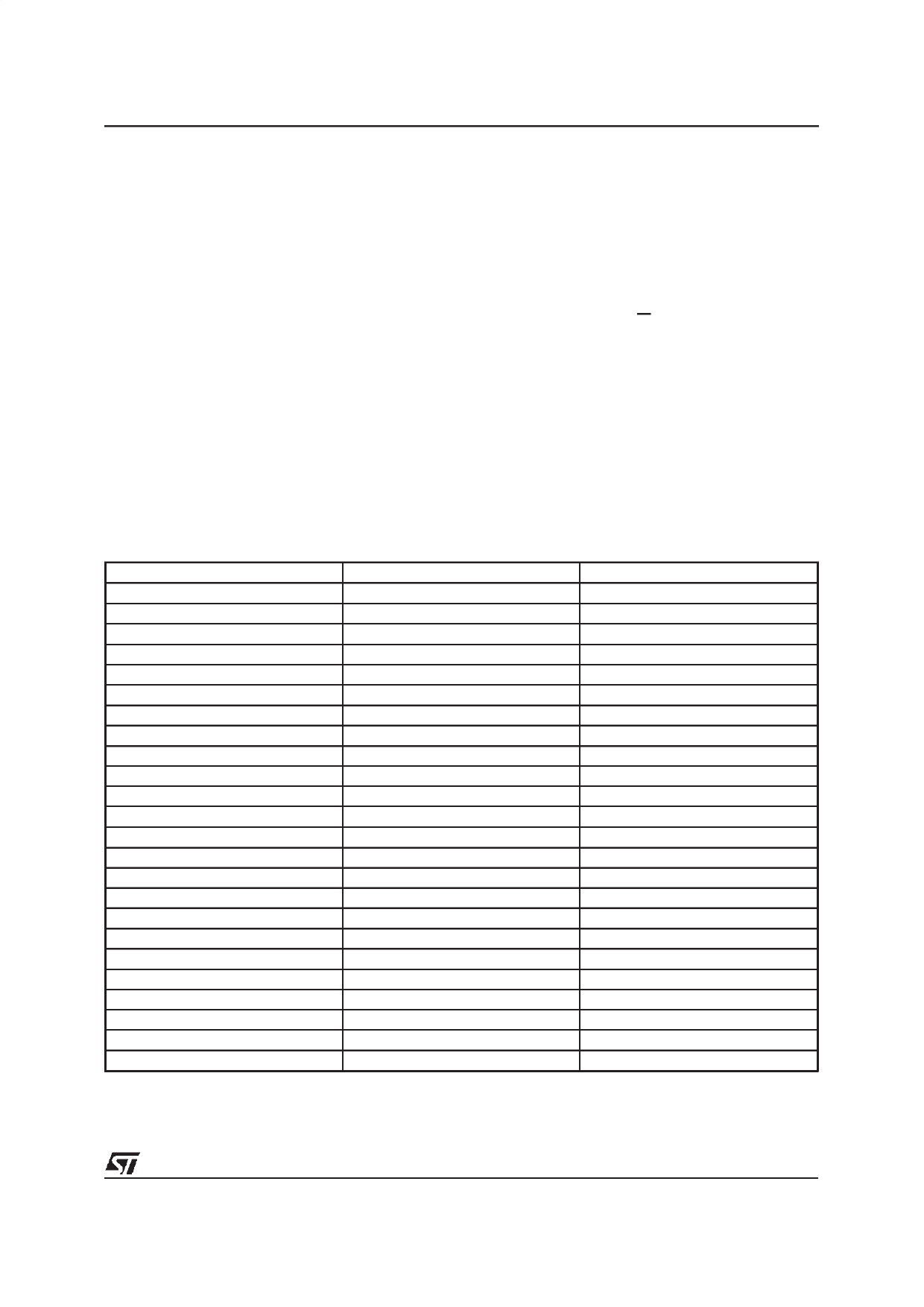
TABLE 1 - ST5451 Internal Registers
Address Hexa
00
1F
20
21
22
23
24
25
26
27
28
29
2A
2B
2C
2D
2E
2F
30
31
32
33
34
3E
Read
Receive FIFO
-
ISTA0
ISTA1
ISTA2
STAR
MODE
RFBC
CA
CB
CC
CD
CE
CF
CIR1
CIR2
MONR1
-
MONR2
-
-
-
-
CCR
Write
Transmit FIFO
-
ISTA0
ISTA1
ISTA2
CMDR
MODE
TSR
CA
CB
CC
CD
CE
CF
CIX1
CIX2
MONX1/0
MONX1/1
MONX2/0
MONX2/1
MASK0
MASK1
MASK2
CCR
5/34