SST36VF1601G Ver la hoja de datos (PDF) - Silicon Storage Technology
Número de pieza
componentes Descripción
Fabricante
SST36VF1601G Datasheet PDF : 36 Pages
| |||
Data Sheet
Ready/Busy# (RY/BY#)
The SST36VF160xG include a Ready/Busy# (RY/BY#)
output signal. RY/BY# is an open drain output pin that indi-
cates whether an Erase or Program operation is in
progress. Since RY/BY# is an open drain output, it allows
several devices to be tied in parallel to VDD via an external
pull-up resistor. After the rising edge of the final WE# pulse
in the command sequence, the RY/BY# status is valid.
When RY/BY# is actively pulled low, it indicates that an
Erase or Program operation is in progress. When RY/BY#
is high (Ready), the devices may be read or left in standby
mode.
Byte/Word (BYTE#)
The device includes a BYTE# pin to control whether the
device data I/O pins operate x8 or x16. If the BYTE# pin is
at logic “1” (VIH) the device is in x16 data configuration: all
data I/0 pins DQ0-DQ15 are active and controlled by CE#
and OE#.
If the BYTE# pin is at logic ‘0’, the device is in x8 data con-
figuration -- only data I/O pins DQ0-DQ7 are active and con-
trolled by CE# and OE#. The remaining data pins DQ8-
DQ14 are at Hi-Z, while pin DQ15 is used as the address
input A-1 for the Least Significant Bit of the address bus.
Data# Polling (DQ7)
When the SST36VF160xG are in an internal Program
operation, any attempt to read DQ7 will produce the com-
plement of true data. Once the Program operation is com-
pleted, DQ7 will produce valid data.
During internal Erase operation, any attempt to read DQ7
will produce a ‘0’. Once the internal Erase operation is com-
pleted, DQ7 will produce a ‘1’. The Data# Polling is valid
after the rising edge of fourth WE# (or CE#) pulse for Pro-
gram operation. For Sector-, Block-, or Chip-Erase, the
Data# Polling is valid after the rising edge of sixth WE# (or
CE#) pulse. See Figure 12 for Data# Polling (DQ7) timing
diagram and Figure 26 for a flowchart.
16 Mbit Concurrent SuperFlash
SST36VF1601G / SST36VF1602G
Toggle Bits (DQ6 and DQ2)
During the internal Program or Erase operation, any con-
secutive attempts to read DQ6 will produce alternating ‘1’s
and ‘0’s, i.e., toggling between ‘1’ and ‘0’. When the internal
Program or Erase operation is completed, the DQ6 bit will
stop toggling, and the device is then ready for the next
operation. For Sector-, Block-, or Chip-Erase, the toggle bit
(DQ6) is valid after the rising edge of sixth WE# (or CE#)
pulse. DQ6 will be set to ‘1’ if a Read operation is attempted
on an Erase-Suspended Sector or Block. If Program oper-
ation is initiated in a sector/block not selected in Erase-Sus-
pend mode, DQ6 will toggle.
An additional Toggle Bit is available on DQ2, which can be
used in conjunction with DQ6 to check whether a particular
sector or block is being actively erased or erase-sus-
pended. Table 2 shows detailed bit status information. The
Toggle Bit (DQ2) is valid after the rising edge of the last
WE# (or CE#) pulse of Write operation. See Figure 13 for
Toggle Bit timing diagram and Figure 26 for a flowchart.
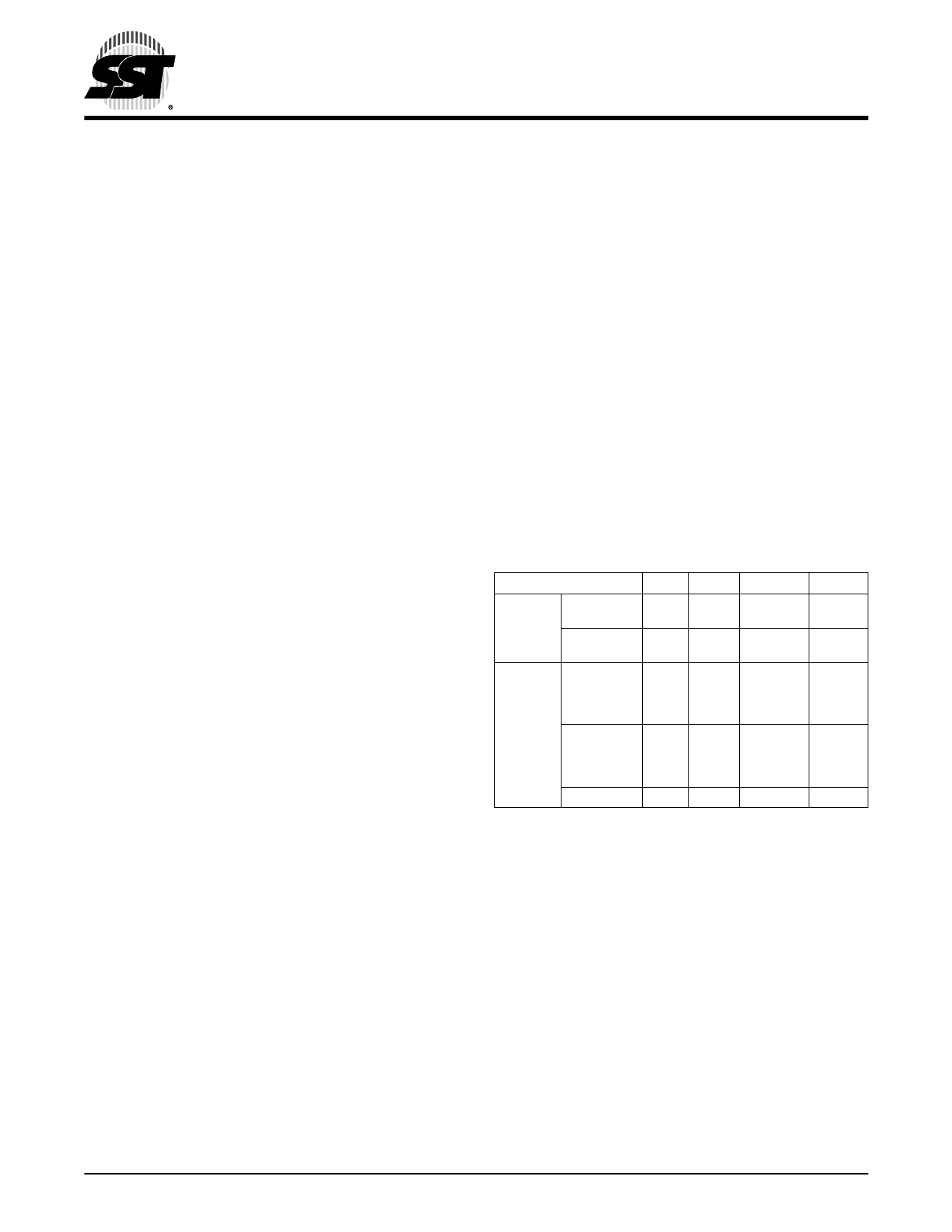
TABLE 2: Write Operation Status
Status
DQ7 DQ6
DQ2
RY/BY#
Normal Standard
DQ7# Toggle No Toggle
0
Operation Program
Standard
0 Toggle Toggle
0
Erase
Erase- Read From
1
1
Toggle
1
Suspend Erase
Mode
Suspended
Sector/Block
Read From Data Data
Data
1
Non-Erase
Suspended
Sector/Block
Program
DQ7# Toggle
N/A
0
T2.1 1342
Note: DQ7, DQ6, and DQ2 require a valid address when reading
status information. The address must be in the bank where
the operation is in progress in order to read the operation sta-
tus. If the address is pointing to a different bank (not busy),
the device will output array data.
©2006 Silicon Storage Technology, Inc.
4
S71342-00-000
12/06
Share Link: 