SST25VF020-20-4C-S2A Ver la hoja de datos (PDF) - Silicon Storage Technology
Número de pieza
componentes Descripción
Fabricante
SST25VF020-20-4C-S2A Datasheet PDF : 24 Pages
| |||
Data Sheet
PRODUCT IDENTIFICATION
TABLE 2: PRODUCT IDENTIFICATION
Manufacturer’s ID
Device ID
SST25VF020
SST25VF040
Address
00000H
00001H
00001H
Data
BFH
43H
44H
T2.0 1231
MEMORY ORGANIZATION
The SST25VF020/040 SuperFlash memory array is orga-
nized in 4 KByte sectors with 32 KByte overlay blocks.
2 Mbit / 4 Mbit SPI Serial Flash
SST25VF020 / SST25VF040
DEVICE OPERATION
The SST25VF020/040 is accessed through the SPI (Serial
Peripheral Interface) bus compatible protocol. The SPI bus
consist of four control lines; Chip Enable (CE#) is used to
select the device, and data is accessed through the Serial
Data Input (SI), Serial Data Output (SO), and Serial Clock
(SCK).
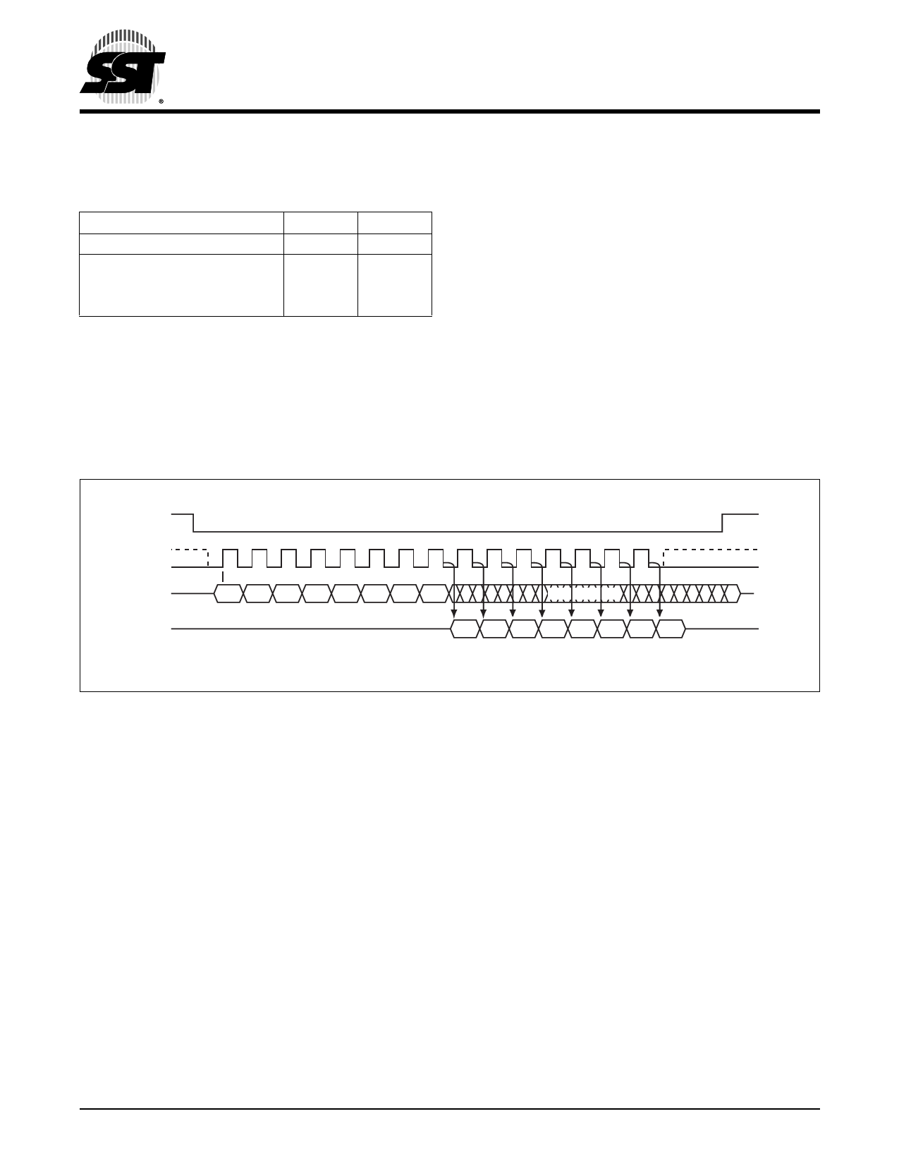
The SST25VF020/040 supports both Mode 0 (0,0) and
Mode 3 (1,1) of SPI bus operations. The difference
between the two modes, as shown in Figure 2, is the state
of the SCK signal when the bus master is in Stand-by
mode and no data is being transferred. The SCK signal is
low for Mode 0 and SCK signal is high for Mode 3. For both
modes, the Serial Data In (SI) is sampled at the rising edge
of the SCK clock signal and the Serial Data Output (SO) is
driven after the falling edge of the SCK clock signal.
CE#
MODE 3
SCK MODE 0
MODE 3
MODE 0
SI
Bit 7 Bit 6 Bit 5 Bit 4 Bit 3 Bit 2 Bit 1 Bit 0
DON'T CARE
MSB
HIGH IMPEDANCE
SO
Bit 7 Bit 6 Bit 5 Bit 4 Bit 3 Bit 2 Bit 1 Bit 0
MSB
1231 F02.1
FIGURE 2: SPI PROTOCOL
©2004 Silicon Storage Technology, Inc.
4
S71231-04-000
6/04
Share Link: 