SPX1582 Ver la hoja de datos (PDF) - Signal Processing Technologies
Número de pieza
componentes Descripción
Fabricante
SPX1582
Signal Processing Technologies

SPX1582 Datasheet PDF : 7 Pages
| |||
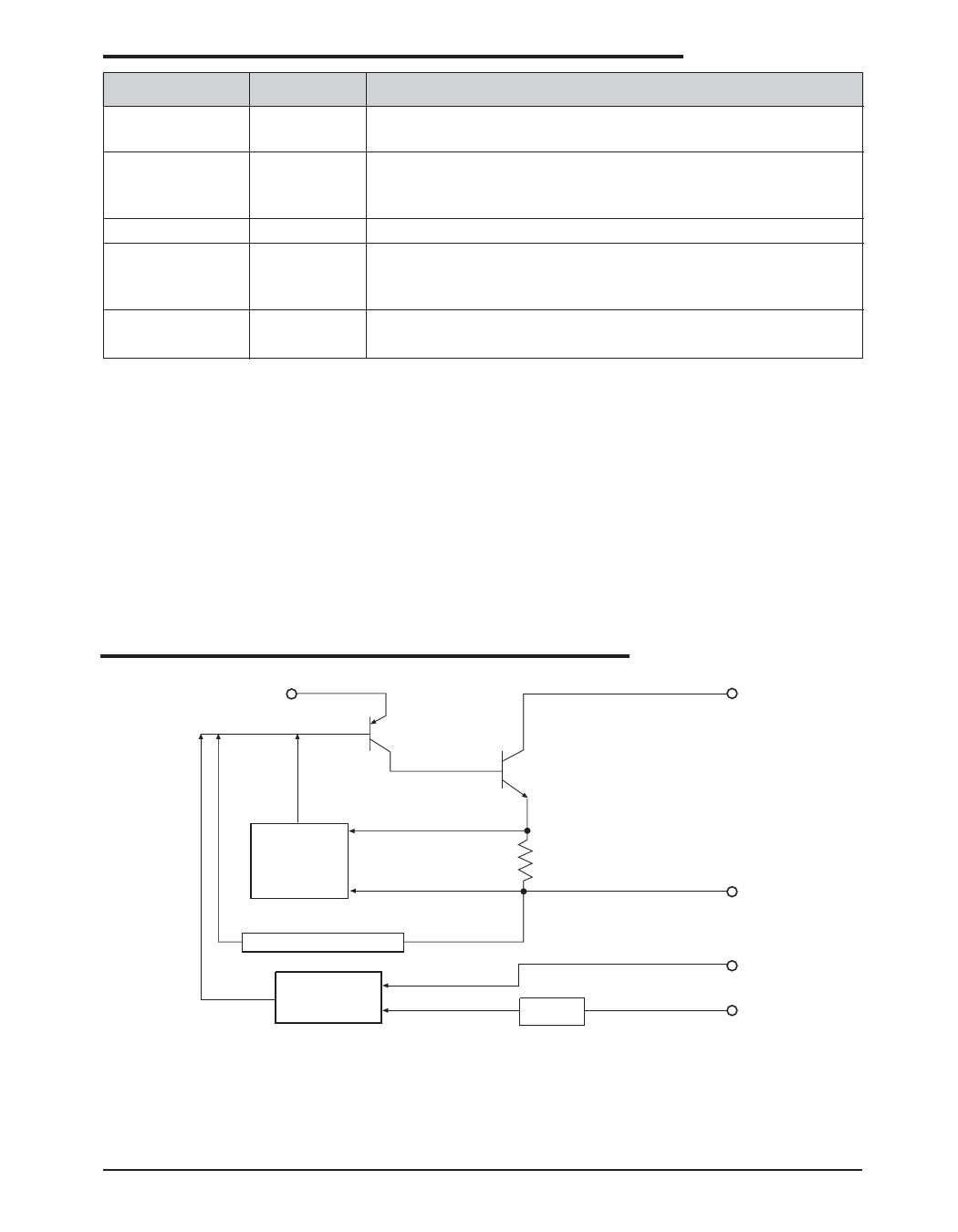
PIN NUMBER
1
2
3
4
5
PIN DESCRIPTION
PIN NAME
SENSE
ADJ
VOUT
VCTRL
VIN
DESCRIPTION
Allows Kelvin sense of VOUT at the load. (Positive side of the
reference voltage of the device).
Negative side of the reference voltage for the device. Adding a small
bypass capacitor from the ADJ pin to ground will improve the transient
response.
Power output of the device.
Supply pin for the control circuitry of the device. The current flow into this
pin will be about 1% of the output current. VCTRL must be between 1.0V
and 1.3V greater than the output voltage for the device to regulate.
Output load current is supplied through this pin. VIN must be between 0.1V
and 0.8V greater than the output voltage for this device to regulate.
Note that TAB is internally connected to Pin 3.
(4) VCTRL
FUNCTIONAL DIAGRAM
VIN (5)
CURRENT
LIMIT
AMPLIFIER
LIMIT
SENSE
THERMAL OVERLOAD
VOLTAGE
REGULATION
AMPLIFIER
VREF
VOUT (3)
SENSE (1)
ADJ (2)
Jun 17-06 Rev F
SPX1582 3A Ultra Low Dropout Voltage Regulator
3
© 2006 Sipex Corporation
Share Link: