SP8126 Ver la hoja de datos (PDF) - Signal Processing Technologies
Número de pieza
componentes Descripción
Fabricante
SP8126 Datasheet PDF : 8 Pages
| |||
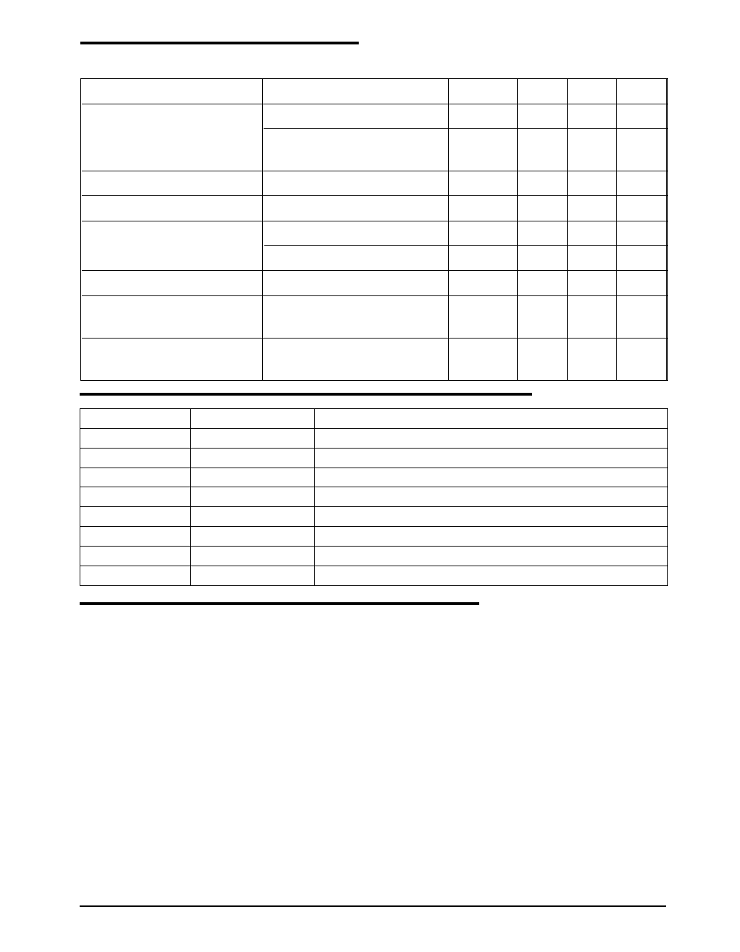
ELECTRICAL SPECIFICATIONS: Continued
Unless otherwise noted: VCC = 5.0V, CLOAD = 50pF to GND, RLOADP = RLOADN = 1kΩ to GND, RGAIN = 510Ω
(Nominal Gain), -20°C ≤ TA ≤ +85°C, Output measured differentially.
PARAMETER
CONDITIONS
MIN TYP MAX UNITS
Output Settling Time (780nm) 2VPP Step
10
13
ns
(1% of Final Value)
2VPP Step,
RGAIN = 1230Ω (High Gain)
15
18
ns
Output Slew Rate
200 300
V/µs
Output Overshoot
2VPP Step
5
%
Power Supply Current
15
mA
-20°C < TA < +85°C
20
mA
Gain Adjust Range
225Ω < RGAIN < 1230Ω
-6
6
dB
Gain Select Input Voltage
VIL (TTL Level)
0.8
V
Gain Select Input Voltage
VIH (TTL Level)
2.0
V
PIN DESCRIPTION
PIN NUMBER
1
2
3
4
5
6
7
8
NAME
VCC
GAIN
RGCOM
GND
RGAIN1
RGAIN2
VOUT-
VOUT+
FUNCTION
Supply Voltage
Gain Select
Common connection point for RGAIN1 and RGAIN2
Power Ground
Gain Adjust 1 (Gain Select = LOW) or OPEN
Gain Adjust 2 (Gain Select = HIGH)
Output Voltage -
Output Voltage +
Internal Operation
The SP8126B APC circuit has an integrated
photo detector and is designed with nominal
sensitivities of 3mV/µW for both 650nm and
780nm wavelength laser light. The part's sensi-
tivity can also be adjusted continuously and
independently for two different gain modes via
two external resistors over a range of ±6dB. The
two gain modes are controlled by a TTL com-
patible logic input, called GAIN SELECT. This
logic pin selects between the two external gain
setting resistors to allow independent control
and settings for the two gain functions.
The system is a two stage design, consisting of
a Trans-Impedance Amplifier (TIA) and an out-
put buffer stage. In dark condition the outputs
VOUT- and VOUT+ are set to a reference voltage
THEORY OF OPERATION
that is defined internally as Vcc/2. With 650nm
or 780nm wavelength laser light falling on the
photodetector, the output will swing differen-
tially around Vcc/2 proportional with the light
power according to the chosen gain.
TIA and Gain control
The first stage is a differential TIA used to
convert the photodetector current to a balanced
differential voltage. The traditional fixed feed-
back resistors have been replaced with an active
resistor circuit that sets the trans-impedance value.
A Resistor Control Block that senses the value
of the external gain setting resistor controls the
value of the equivalent feedback resistor.
Rev:B Date: 3/18/04
SP8126B High Speed Differential APC Amplifier
3
© Copyright 2004 Sipex Corporation
Share Link: 