SP8110 Ver la hoja de datos (PDF) - Signal Processing Technologies
Número de pieza
componentes Descripción
Fabricante
SP8110 Datasheet PDF : 3 Pages
| |||
Advance
SP8110
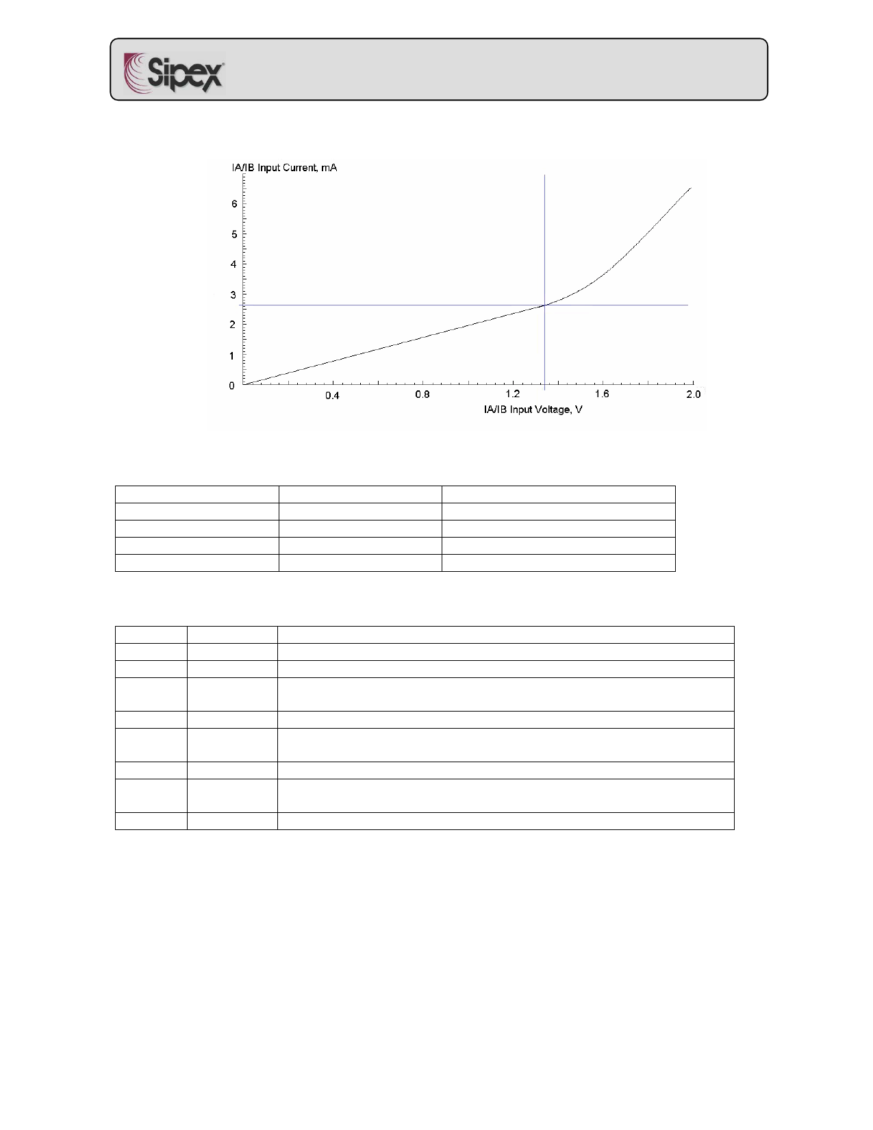
INPUT CHARACTERISTICS: IA/IB INPUT CURRENT VS INPUT VOLTAGE
MODE SELECTION
IA current
> 2.65 mA
< 2.5 mA
> 2.65 mA
< 2.5 mA
IB current
< 2.5 mA
> 2.65 mA
> 2.65 mA
< 2.5 mA
Mode
LD_A output active
LD_B output active
Error
Power Save
PIN ASSIGNMENTS
Pin No.
1
2
3
4
5
6
7
8
Pin Name
IA
IB
RFreq
Vcc
LD_B
GND
LD_A
Vcc_out
Function
Amplitude setting for output LD_A
Amplitude setting for output LD_B
Modulation Frequency adjusting pin
(An external resistor is connected between this pin and ground.)
Power supply pin
Output pin of channel B
(Anode of laser diode is connected with this pin.)
Ground pin
Output pin of channel A
(Anode of laser diode is connected with this pin.)
Power supply for LD_A and LD_B outputs
BOARD LAYOUT AND GROUNDING
To obtain the best performance from the SP8110, a printed circuit board with ground plane is
required. High quality, low series resistance ceramic 0.1uF bypass capacitors should be used at
the Vcc and Vcc_out pins (pins 4 and 8). Pin 8 should also have a 0.1uF bypass capacitor.
These capacitors must be located as close to the pins as possible. The traces connecting the
pins and the bypassing capacitors must be kept short and should be made as wide as possible.
Rev 0.1 (12-03-03): SP8110 – Two-Channel Modulation IC
SIPEX RESERVES THE RIGHT TO MAKE CHANGES TO THIS DATASHEET. CALL FOR UPDATES: 1-978-667-8700.
SIPEX CONFIDENTIAL, PRELIMINARY & PROPRIETARY. DO NOT DISTRIBUTE
OR COPY
page 2 of 3
Share Link: 