SP3220B Ver la hoja de datos (PDF) - Signal Processing Technologies
Número de pieza
componentes Descripción
Fabricante
SP3220B Datasheet PDF : 18 Pages
| |||
Receivers
The receiver converts EIA/TIA-232 levels to
TTL or CMOS logic output levels. The receiver
has an inverting high-impedance output. This
receiver output (RxOUT) is at high-impedance
when the enable control EN = HIGH. In the
shutdown mode, the receiver can be active or
inactive. EN has no effect on TxOUT. The truth
table logic of the SP3220B/U driver and receiver
outputs can be found in Table 2.
Since receiver input is usually from a transmission
line where long cable lengths and system
interference can degrade the signal, the inputs
have a typical hysteresis margin of 300mV.
This ensures that the receiver is virtually
immune to noisy transmission lines. Should an
input be left unconnected, a 5kΩ pulldown
resistor to ground will commit the output of the
receiver to a HIGH state.
Charge Pump
The charge pump is a Sipex–patented design
(U.S. 5,306,954) and uses a unique approach
compared to older less–efficient designs. The
charge pump still requires four external
capacitors, but uses a four–phase voltage shifting
technique to attain symmetrical 5.5V power
supplies. The internal power supply consists of
a regulated dual charge pump that provides
output voltages 5.5V regardless of the input
voltage (V ) over the +3.0V to +5.5V range.
CC
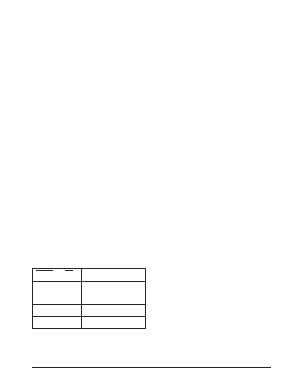
SHDN EN TxOUT RxOUT
0
0
Tri-state Active
0
1
Tri-state Tri-state
1
0
Active
Active
1
1
Active Tri-state
Table 2. Truth Table Logic for Shutdown and
Enable Control
In most circumstances, decoupling the power
supply can be achieved adequately using a 0.1µF
bypass capacitor at C5 (refer to Figures 11).
In applications that are sensitive to power-
supply noise, decouple VCC to ground with a
capacitor of the same value as charge-pump
capacitor C1. Physically connect bypass
capacitors as close to the IC as possible.
The charge pumps operate in a discontinuous
mode using an internal oscillator. If the output
voltages are less than a magnitude of 5.5V, the
charge pumps are enabled. If the output voltage
exceed a magnitude of 5.5V, the charge pumps
are disabled. This oscillator controls the four
phases of the voltage shifting. A description of
each phase follows.
Phase 1
— VSS charge storage — During this phase of
the clock cycle, the positive side of capacitors
C and C are initially charged to V . C + is then
1
2
CC l
switched to GND and the charge in C1– is
transferred to C2–. Since C2+ is connected to VCC,
the voltage potential across capacitor C2 is now
2 times VCC.
Phase 2
— VSS transfer — Phase two of the clock
connects the negative terminal of C to the V
2
SS
storage capacitor and the positive terminal of C2
to GND. This transfers a negative generated
voltage to C3. This generated voltage is
regulated to a minimum voltage of -5.5V.
Simultaneous with the transfer of the voltage to
C3, the positive side of capacitor C1 is switched
to VCC and the negative side is connected to GND.
Phase 3
— V charge storage — The third phase of the
DD
clock is identical to the first phase — the charge
transferred in C1 produces –VCC in the negative
terminal of C , which is applied to the negative
1
side of capacitor C2. Since C2+ is at VCC, the
voltage potential across C2 is 2 times VCC.
Rev. 7/8/03
SP3220B/U +3.0 to +5.0V RS-232 Transceivers
11
© Copyright 2003 Sipex Corporation
Share Link: 