SP3012 Ver la hoja de datos (PDF) - Littelfuse, Inc
Número de pieza
componentes Descripción
Fabricante
SP3012 Datasheet PDF : 6 Pages
| |||
TVS Diode Arrays (SPA® Diodes)
Low Capacitance ESD Protection - SP3012 Series
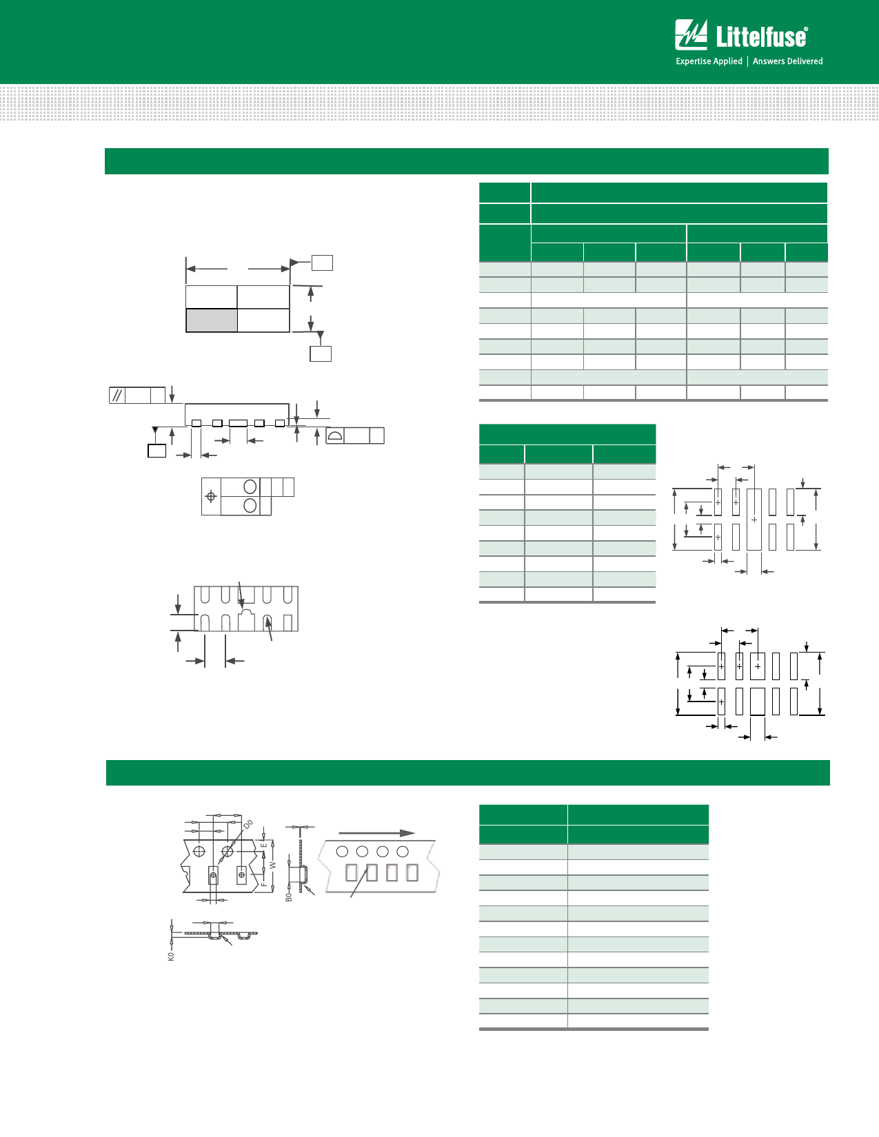
Package Dimensions— µDFN-10 (2.5x1.0x0.5mm)
Top View
D
A
E
0.05 C
A
Seating
Plane
C
Side View
B
A1 A3
b1
b
0.05 C
0.10 M C A B
0.05 M C
Bottom View
R0.125
L
2xR0.075mm (7x)
e
Recomended
Soldering Pad Layout
P1
P
Embossed Carrier Tape & Reel YSpecification— µDFN-10
Z (C) G
(Y1)
P0
P1
P2
D0
X
X1
T User Feeding Direction
D1
A0
5º Max
5º Max Pin 1 Location
Top View
D
A
E
Package
JEDEC
Symbol
A
A1
A3
b
b1
D
E
e
L
B
0.05 C
Side View
µDFSNea-t1in0g(2.5x1A.0x0.5mm)
PlaneMO-229
C
Millimeters
b1
b
Inches
A1 A3
0.05 C
Min
Nom
Max
Min 0.10NMomC A B Max
0.48
0.515
0.55
0.019 0.050M.02C0 0.021
0.00
--
0.05
0.000
0.022
0.125 Ref
0.15
0.20
0.25
0.35
0.40
0.45
0.005 Ref
0.006Botto0m.0V08iew 0.012
0.014 R0.1205.016 0.018
2.40
2.50
2.60
0.094 0.098 0.102
0.90
1.00
1.10
0.035 0.039 0.043
L
0.50 BSC
0.020 BSC
0.30
0.365
0.43
0.012 2x0R.001.0475mm0.0(71x6)
e
Soldering Pad Layout Dimensions
Inch
Millimeter
C
(0.034)
(0.875)
G
0.008
0.20
P
0.020
0.50
P1
0.039
1.00
X
0.008
0.20
X1
0.016
0.40
Y
0.027
0.675
Y1
(0.061)
(1.55)
Z
0.061
1.55
Recomended
Soldering Pad Layout
P1
P
Z (C) G
Y
(Y1)
X
X1
Alternative
Soldering Pad Layout
P1
P
Z (C) G
Y
(Y1)
X
X1
Package
Symbol
A0
B0
D0
D1
E
F
K0
P0
P1
P2
T
W
µDFN-10 (2.5x1.0x0.5mm)
Millimeters
1.30 ± 0.10
2.83 ± 0.10
Ø 1.50 + 0.10
Ø 1.00 + 0.25
1.75 ± 0.10
3.50 ± 0.05
0.65 ± 0.10
4.00 ± 0.10
4.00 ± 0.10
2.00 ± 0.05
0.254 ± 0.02
8.00 + 0.30 /- 0.10
© 2013 Littelfuse, Inc.
Specifications are subject to change without notice.
Revised: 04/24/13
Share Link: 