SP204 Ver la hoja de datos (PDF) - Signal Processing Technologies
Número de pieza
componentes Descripción
Fabricante
SP204 Datasheet PDF : 16 Pages
| |||
VCC = +5V
+
C1 –
–5V
+5V
+
C2 –
–5V
C4
+ – VDD Storage Capacitor
– + VSS Storage Capacitor
C3
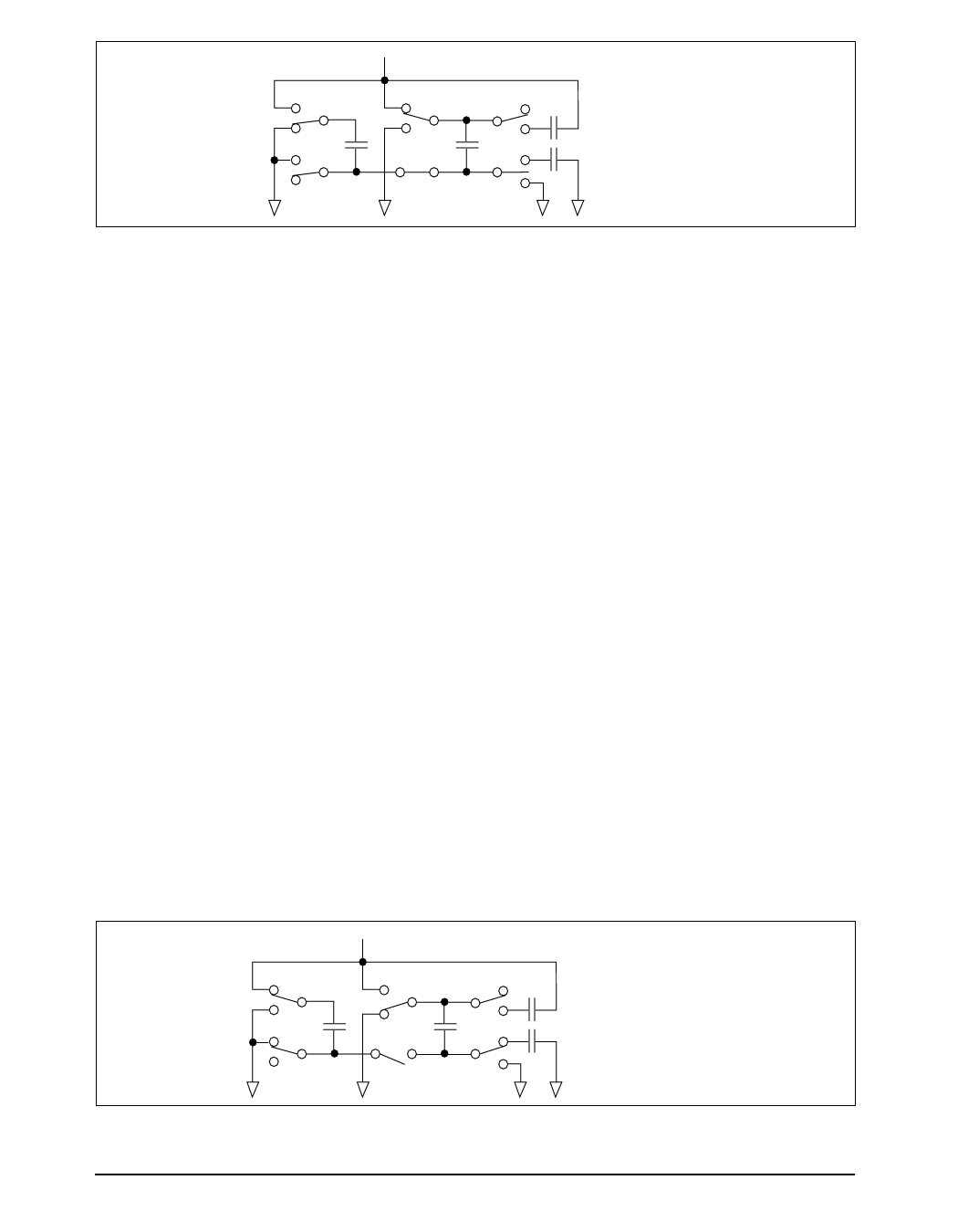
Figure 1. Charge Pump — Phase 1
attain symmetrical ±10V power supplies.
Figure 3a shows the waveform found on the
positive
side
of
capcitor
C,
2
and
Figure
3b
shows the negative side of capcitor C2. There is
a free–running oscillator that controls the four
phases of the voltage shifting. A description of
each phase follows.
Phase 1
— V charge storage —During this phase of the
SS
clock cycle, the positive side of capacitors C1
and C are initially charged to +5V. C + is then
2
l
switched to ground and the charge in C – is
1
transferred to C –. Since C + is connected to
2
2
+5V, the voltage potential across capacitor C2 is
now 10V.
Phase 2
— VSS transfer — Phase two of the clock con-
nects the negative terminal of C2 to the VSS
storage capacitor and the positive terminal of C2
to ground, and transfers the generated –l0V to
C3. Simultaneously, the positive side of capaci-
tor C 1 is switched to +5V and the negative side
is connected to ground.
Phase 3
— VDD charge storage — The third phase of the
clock is identical to the first phase — the charge
VCC = +5V
transferred in C1 produces –5V in the negative
terminal of C1, which is applied to the negative
side of capacitor C2. Since C2+ is at +5V, the
voltage potential across C2 is l0V.
Phase 4
— VDD transfer — The fourth phase of the clock
connects the negative terminal of C to ground,
2
and transfers the generated l0V across C to C ,
2
4
the VDD storage capacitor. Again, simultaneously
with this, the positive side of capacitor C1 is
switched to +5V and the negative side is con-
nected to ground, and the cycle begins again.
Since both V+ and V– are separately generated
from VCC; in a no–load condition V+ and V– will
be symmetrical. Older charge pump approaches
that generate V– from V+ will show a decrease in
the magnitude of V– compared to V+ due to the
inherent inefficiencies in the design.
The clock rate for the charge pump typically
operates at 15kHz. The external capacitors can
be as low as 0.1µF with a 16V breakdown
voltage rating.
The SP200 Series devices are made up of three
basic circuit blocks — 1) transmitter/driver, 2)
receiver and 3) the Sipex proprietary charge
+
C1 –
+
C2 –
–10V
C4
+ – VDD Storage Capacitor
– + VSS Storage Capacitor
C3
Figure 2. Charge Pump — Phase 2
Date:03/04/2005
+5V High-Speed RS232 Transceivers
6
© Copyright 2005 Sipex Corporation
Share Link: 