SP204 Ver la hoja de datos (PDF) - Signal Processing Technologies
Número de pieza
componentes Descripción
Fabricante
SP204 Datasheet PDF : 16 Pages
| |||
VCC .................................................................................................. +6V
V+ ...................................................................... (VCC – 0.3V) to +13.2V
V– ................................................................................................ 13.2V
Input Voltages
TIN ......................................................................... –0.3V to (VCC +0.3V)
RIN ................................................................................................ ±20V
Output Voltages
TOUT ............................................................... (V+, +0.3V) to (V–, –0.3V)
ROUT ...................................................................... –0.3V to (VCC +0.3V)
Short Circuit Duration on TOUT ............................................ Continuous
Power Dissipation
Plastic DIP ............................................................................... 375mW
(derate 7mW/°C above +70°C)
Small Outline ............................................................................ 375mW
(derate 7mW/°C above +70°C)
ABSOLUTE MAXIMUM RATINGS
These are stress ratings only and functional operation of the device at
these or any other above those indicated in the operation sections of the
specifications below is not implied. Exposure to absolute maximum rating
conditions for extended periods of time may affect reliability.
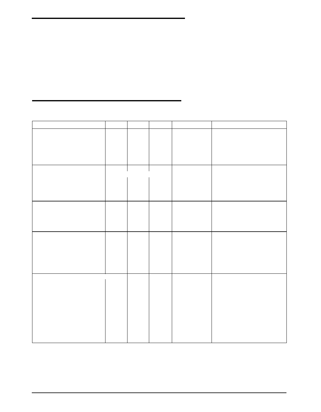
ELECTRICAL CHARACTERISTICS
VCC at nominal ratings; 0.1µF charge pump capacitors; TMIN to TMAX, unless otherwise noted.
PARAMETER
TTL INPUTS
Logic Threshold
VIL
VIH
Logic Pullup Current
Maximum Data Rate
TTL OUTPUTS
Compatibility
VOL
VOH
Leakage Current
MIN. TYP. MAX.
0.8
2.0
15
200
120
TTL/CMOS
0.4
3.5
0.05
±10
RS-232 OUTPUT
Output Voltage Swing
±5
±7
Output Resistance
300
Output Short Circuit Current
±25
RS-232 INPUT
Voltage Range
Voltage Threshold
LOW
HIGH
Hysteresis
Resistance
–15
+15
0.8
1.2
1.7
2.4
0.2
0.5
1.0
3
5
7
DYNAMIC CHARACTERISTICS
Propagation Delay
Instantaneous Slew Rate
1.5
30
Transition Region Slew Rate
5
Output Enable Time
400
Output Disable Time
250
UNIT
Volts
Volts
µA
kbps
CONDITIONS
TIN, EN, SD
TIN = 0V
CL = 2,500pF, RL = 3kΩ
Volts
Volts
µA
Volts
Ohms
mA
Volts
Volts
Volts
Volts
kΩ
µs
V/µs
V/µs
ns
ns
IOUT = 3.2mA; VCC = +5V
IOUT = –1.0mA
EN = VCC; 0V ≤ VOUT ≤ VCC ;
TA = +25°C
All transmitter outputs loaded
with 3kΩ to ground
VCC = 0V; VOUT = ±2V
Infinite duration
VCC = 5V, TA = +25°C
VCC = 5V, TA = +25°C
VCC = +5V
±15V; TA = +25°C
RS-232–to–TTL
CL = 50pF, RL = 3–7kΩ;
TA = +25°C
CL = 2,500pF, RL = 3kΩ;
measured from +3V to –3V
or –3V to +3V
Date:03/04/2005
+5V High-Speed RS232 Transceivers
2
© Copyright 2005 Sipex Corporation
Share Link: 