SP1085 Ver la hoja de datos (PDF) - Signal Processing Technologies
Número de pieza
componentes Descripción
Fabricante
SP1085 Datasheet PDF : 12 Pages
| |||
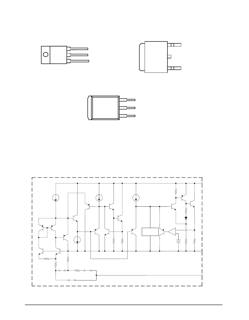
Pin configuration
V Package
(TO-220)
3
2
1
INPUT
OUTPUT
ADJ/GND
V1 Package
(TO-263-3L)
3
2
1
V2 Package
(TO-252)
3
2
1
INPUT
OUTPUT
ADJ/GND
INPUT
OUTPUT
ADJ/GND
Figure 2. Pin Configuration of SP085 (Top View)
functional Block Diagram
INPUT
Thermal
-
Protection
+
A
B
Date: 7/24/06 Rev H
OUTPUT
For Adjustable Output, disconnect A and A2, connect B
A2
For Fixed Output, connect A and A2, disconnect B
ADJ/
GND
Figure 3. Functional Block Diagram of SP085
SP1085 3A Low Dropout Linear Regulator
© 2006 Sipex Corporation
Share Link: 