MX803ALH Ver la hoja de datos (PDF) - MX-COM Inc
Número de pieza
componentes Descripción
Fabricante
MX803ALH Datasheet PDF : 26 Pages
| |||
Audio Signaling Processor
2. Signal List
4
MX803A PRELIMINARY INFORMATION
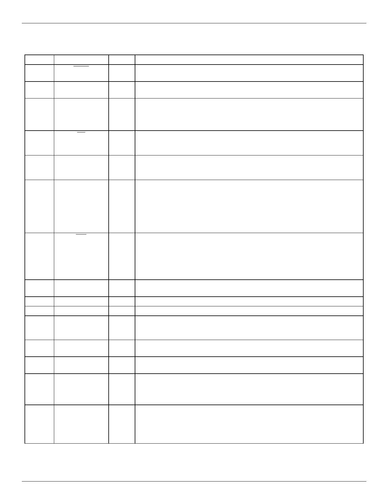
Pin No.
1
2
3
4
5
6
7
10
11
12
13
14
15
16
17
Name
XTAL
Xtal/Clock
Reply Data
CS
Command Data
Logic Input
IRQ
Audio Switch In
Audio Switch Out
VSS
Rx Audio In
Signal Input Bias
VBIAS
Tone 1 Out
Tone 2 Out
Type
Output
Input
Output
Input
Input
Input
Output
Input
Output
Power
Input
Input
Output
Output
Output
Description
Output of the on-chip clock oscillator. External components are required at this
output when a Xtal is used. See Figure 2.
Input to the on-chip clock oscillator inverter. A Xtal or externally derived clock
should be connected here. See Figure 2.
C-BUS serial data output to the µC. The transmission of Reply Data bytes is
synchronized to the Serial Clock under the control of the Chip Select input.
This 3-state output is held at high impedance when not sending data to the µC.
See Figure 8 and Figure 9.
C-BUS data loading control function. This input is provided by the µC. Data
transfer sequences are initiated, completed or aborted by the chip select signal.
See Figure 8 and Figure 9.
C-BUS serial data input from the µC. Data is loaded to this device in 8-bit
bytes, MSB (B7) first and LSB (B0) last, synchronized to the Serial Clock. See
Figure 8 and Figure 9.
This “real-time” input is available as a general purpose logic input port which
can be read from the Status Register. See Table 3.
G/Purpose Timer Period Expired
NOTONE Timer Period Expired
RX Tone Measurement Complete
These interrupts are inactive during relevant powersave conditions and can be
disabled by bits 5 and 6 in the Control Register.
Output of this pin indicates an interrupt condition to the µC by going to a logic
“0.” This is a “wire-or-able” output, allowing the connection of up to 8
peripherals to 1 interrupt port on the µC. This pin has a low impedance
pulldown to logic “0” when active and a high impedance when inactive. The
system IRQ line requires one pullup resistor to VDD. The conditions that cause
interrupts are indicated in the Status Register and are shown below:
Input to the stand-alone on-chip Audio Switch. This function is
enabled/disabled by Bit 7 of the Control Register
Output of the stand-alone on-chip Audio Switch..
Negative supply (GND).
Received audio tone signaling input. This input must be ac coupled and
connected, using external components, to the Signal Input Bias pin. See Figure
2.
External components are required between this input and the RX Audio In pin.
See Figure 2.
Internal circuitry bias signal, held at VDD/2. This pin should be decoupled to VSS
by capacitor C2. See Figure 2..
Tone 1 Generator (2-/5-tone Selcall or DTMF 1) output. External gain and
coupling components are required at this output when operating in a complete
DBS 800 audio installation. The frequency of this output is determined by
writing to the TX Tone Generator 1 Register (Table 5). See Figure 2.
Tone 2 Generator (2-/5-tone Selcall, CUES or DTMF 2) output. External gain
and coupling components are required at this output when operating in a
complete DBS 800 audio installation. The frequency of this output is
determined by writing to the TX Tone Generator 2 Register (Table 5).
See Figure 2.
© 1996 MX•COM, INC.
Tele: 800 638 5577 910 744 5050 Fax: 910 744 5054
Doc. # 20480122.003
Share Link: 