SPT9210SCS Ver la hoja de datos (PDF) - Signal Processing Technologies
Número de pieza
componentes Descripción
Fabricante
SPT9210SCS Datasheet PDF : 11 Pages
| |||
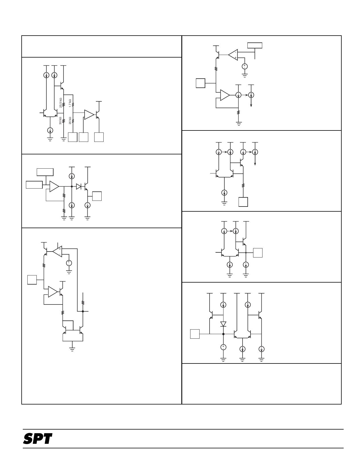
TERMINAL EXPLANATIONS - CONTINUED
VCCVCC VCC
Inner
Voltage
Reference
(2.0 V)
Pin Name
10 Ground
Voltage
0.0 V
Pin Name
11 VRH Adjust
12 VRL Sense
13 VRL Force
Voltage
3.6 V
3.6 V
3.6 V
VCC These terminals are the
Buffer
reference voltage sources for
Amp
the ADC on the high side.
+
-
They are the output, sense
and adjustment terminals.
11 12 13
Clamp
VCC VCC
Pin Name Voltage
14 Output Y 2.5 V
AGC
+
-
6 kΩ
3 kΩ
This terminal is the luminance
14 signal output.
4.8 mA
VCC CLK Signal
Pin Name Voltage
15 C-Clamp Y 0.6 V
10 kΩ
Clamp
Voltage
15
VCC
+
-
2 kΩ
This terminal connects the
capacitor that determines the
time constant of the luminance
clamp circuit.
From
AGC
2 kΩ
To Final
Amp
VCC DLY Signal Clamp
10 kΩ
AGC
Voltage
To Final
Amp
16
VCC VCC
+
-
Pin Name
16 C-AGC
Voltage
0.6 V
This terminal connects the
capacitor that determines the
time constant of the AGC
circuit.
3.6 kΩ
To AGC
VCC VCC VCC VCC
Pin Name Voltage
17 Filter Adjust 0.7 V
V_BG =
1.2 V
To Filter
Control
This terminal is the fc
adjustment of the internal
low pass filter.
7 kΩ
17
VCC VCC VCC
Inner Voltage
Reference
18
(2.0 V)
Pin Name Voltage
18 VRef Clamp 2.0 V
This terminal is the bypass
capacitor connection for the
internal reference voltage
circuit.
VCC VCC VCC VCC VCC Pin
Name
Voltage
19 Input Y/C 2.0 V
This terminal is the input of
the composite signal. The
clamp circuit fixes the sync/
bottom voltage to 2.0 V.
19
V_Clamp =
2.0 V
Pin Name
20
VCC
Voltage
5.0 V
This terminal is the power
supply.
SPT
7
SPT9210
11/7/97
Share Link: 