AN87C196CB-20 Ver la hoja de datos (PDF) - Intel
Número de pieza
componentes Descripción
Fabricante
AN87C196CB-20 Datasheet PDF : 33 Pages
| |||
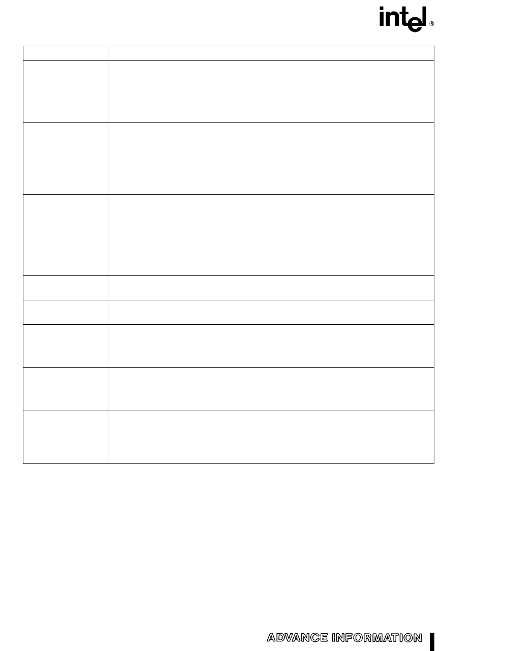
87C196CA 87C196CB
Symbol
P5 7 BUSWIDTH
(CB only)
P5 6 READY
P5 5 BHE WRH
P5 4 SLPINT
P5 3 RD
P5 2 WR WRL
P5 1 INST
(CB only)
P5 0 ALE ADV
Name and Function
Input for bus width selection If CCR bit 1 is a one and CCR1 bit 2 is a one this pin
dynamically controls the Buswidth of the bus cycle in progress If BUSWIDTH is low
an 8-bit cycle occurs if BUSWIDTH is high a 16-bit cycle occurs If CCR bit 1 is ‘‘0’’
and CCR1 bit 2 is ‘‘1’’ all bus cycles are 8-bit if CCR bit 1 is ‘‘1’’ and CCR1 bit 2 is
‘‘0’’ all bus cycles are 16-bit CCR bit 1 e ‘‘0’’ and CCR1 bit 2 e ‘‘0’’ is illegal Also
an LSIO pin when not used as BUSWIDTH
Ready input to lengthen external memory cycles for interfacing with slow or dynamic
memory or for bus sharing If the pin is high CPU operation continues in a normal
manner If the pin is low prior to the falling edge of CLKOUT the memory controller
goes into a wait state mode until the next opositive transition in CLKOUT occurs with
READY high When external memory is not used READY has no effect The max
number of wait states inserted into the bus cycle is controlled by the CCR CCR1
Also an LSIO if READY is not selected
Byte High Enable or Write High output as selected by the CCR BHE e 0 selects
the bank of memory that is connected to the high byte of the data bus A0 e 0
selects the bank of memory that is connected to the low byte Thus accesses to a
16-bit wide memory can be to the low byte only (A0 e 0 BHE e 1) to the high
byte only (A0 e 1 BHE e0) or both bytes (A0 e 0 BHE e 0) If the WRH
function is selected the pin will go low if the bus cycle is writing to an odd memory
location BHE WRH is only valid during 16-bit external Also an LSIO pin when
not BHE WRH
Dual function I O pin As a bidirectional port pin or as a system function The system
function is a Slave Port Interrupt Output Pin (on CA bidirectional port pin only)
Read signal output to external memory RD is active only during external memory
reads or LSIO when not used as RD
Write and Write Low output to external memory as selected by the CCR WR will
go low for every external write while WRL will go low only for external writes where
an even byte is being written WR WRL is active during external memory writes
Also an LSIO pin when not used as WR WRL
Output high during an external memory read indicates the read is an instruction
fetch INST is valid throughout the bus cycle INST is active only during external
memory fetches during internal EPROM fetches INST is held low Also LSIO when
not INST
Address Latch Enable or Address Valid Output as selected by CCR Both pin
options provide a latch to demultiplex the address from the address data bus When
the pin is ADV it goes inactive (high) at the end of the bus cycle ADV can be
used as a chip select for external memory ALE ADV is active only during external
memory accesses Also LSIO when not used as ALE
8
Share Link: 