87C196(1998) Ver la hoja de datos (PDF) - Intel
Número de pieza
componentes Descripción
Fabricante
87C196 Datasheet PDF : 38 Pages
| |||
87C196CA/87C196CB - Express
4.0
PIN DESCRIPTIONS
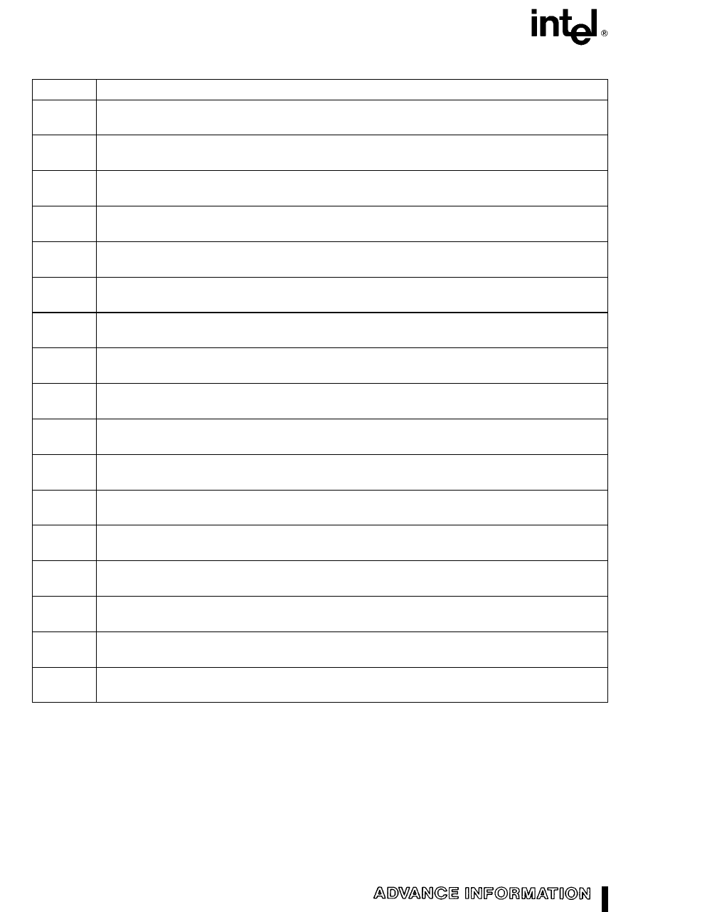
Table 2. Pin Descriptions (Sheet 1 of 3)
Name
VCC
VSS, VSS1
VREF
VPP
ANGND
XTAL1
XTAL2
RESET#
NMI
EA#
PLLEN
(196CB only)
P6.4-6.7/SSIO
P6.3/T1DIR
(CB only)
P6.2/T1CLK
(CB only)
P6.0-6.1/EPA8-9
P5.7/BUSWIDTH
(CB only)
Description
Main supply voltage (+5 V).
Digital circuit ground (0 V). There are seven VSS pins CB (4 on CA), all of which MUST
be connected to a single ground plane.
Reference for the A/D converter (+5 V). VREF is also the supply voltage to the analog
portion of the A/D converter and the logic used to read Port 0. Must be connected for A/D
and Port 0 to function.
Programming voltage for the EPROM parts. It should be +12.5 V for programming. It is
also the timing pin for the return from powerdown circuit. Connect this pin with a 1 µF
capacitor to VSS and a 1 MΩ resistor to VCC. If this function is not used, VPP may be tied
to VCC.
Reference ground for the A/D converter. Must be held at nominally the same potential as
VSS.
Input of the oscillator inverter and the internal clock generator.
Output of the oscillator inverter.
Reset input to the chip. Input low for at least 16 state times resets the chip. The
subsequent low-to-high transition resynchronizes CLKOUT and commences a 10-state
time sequence in which the PSW is cleared, bytes are read from 2018H, 201AH and
201CH (if enabled) loading the CCBs, and a jump to location 2080H is executed. Input
high for normal operation. RESET# has an internal pullup.
A positive transition causes a non-maskable interrupt vector through memory location
203EH. If not used, this pin should be tied to VSS. May be used by Intel Evaluation
boards.
Input for memory select (External Access). EA# equal to a high causes memory
accesses to locations 0FF2000H through 0FFFFFH to be directed to on-chip
EPROM/ROM. EA# equal to a low causes accesses to these locations to be directed to
off- chip memory. EA# = +12.5 V causes execution to begin in the Programming Mode.
EA# latched at reset.
Selects between PLL mode or PLL bypass mode. This pin must be either tied high or
low. PLLEN pin = 0, bypass PLL mode. PLLEN pin = 1, places a 4x PLL at the input of
the crystal oscillator. Allows for a low frequency crystal to drive the device
(i.e., 5 MHz = 16 MHz operation).
Dual-function I/O ports that have a system function as Synchronous Serial I/O. Two pins
are clocks and two pins are data, providing full duplex capability. Also, LSIO when not
used as SSIO.
Dual-function I/O pin. Primary function is that of a bidirectional I/O pin, however, it may
also be used as a TIMER1 Direction input. The TIMER1 increments when this pin is high
and decrements when this pin is low.
Dual-function I/O pin. Primary function is that of a bidirectional I/O pin, however may also
be used as a TIMER1 Clock input. The TIMER1 increments or decrements on both
positive and negative edges of this pin.
Dual-function I/O port pins. Primary function is that of bidirectional I/O. System function is
that of High Speed capture and compare.
Input for bus width selection. If CCR bit 1 is a one and CCR1 bit 2 is a one, this pin
dynamically controls the Buswidth of the bus cycle in progress. If BUSWIDTH is low, an
8-bit cycle occurs, if BUSWIDTH is high, a 16-bit cycle occurs. If CCR bit 1 is “0” and
CCR1 bit 2 is “1”, all bus cycles are 8-bit, if CCR bit 1 is “1” and CCR1 bit 2 is “0”, all bus
cycles are 16-bit. CCR bit 1 = “0” and CCR1 bit 2 = “0” is illegal. Also an LSIO pin when
not used as BUSWIDTH.
6
ADVANCE INFORMATION Datasheet
Share Link: 