SM9403BM Ver la hoja de datos (PDF) - Nippon Precision Circuits
Número de pieza
componentes Descripción
Fabricante
SM9403BM Datasheet PDF : 18 Pages
| |||
SM9403BM
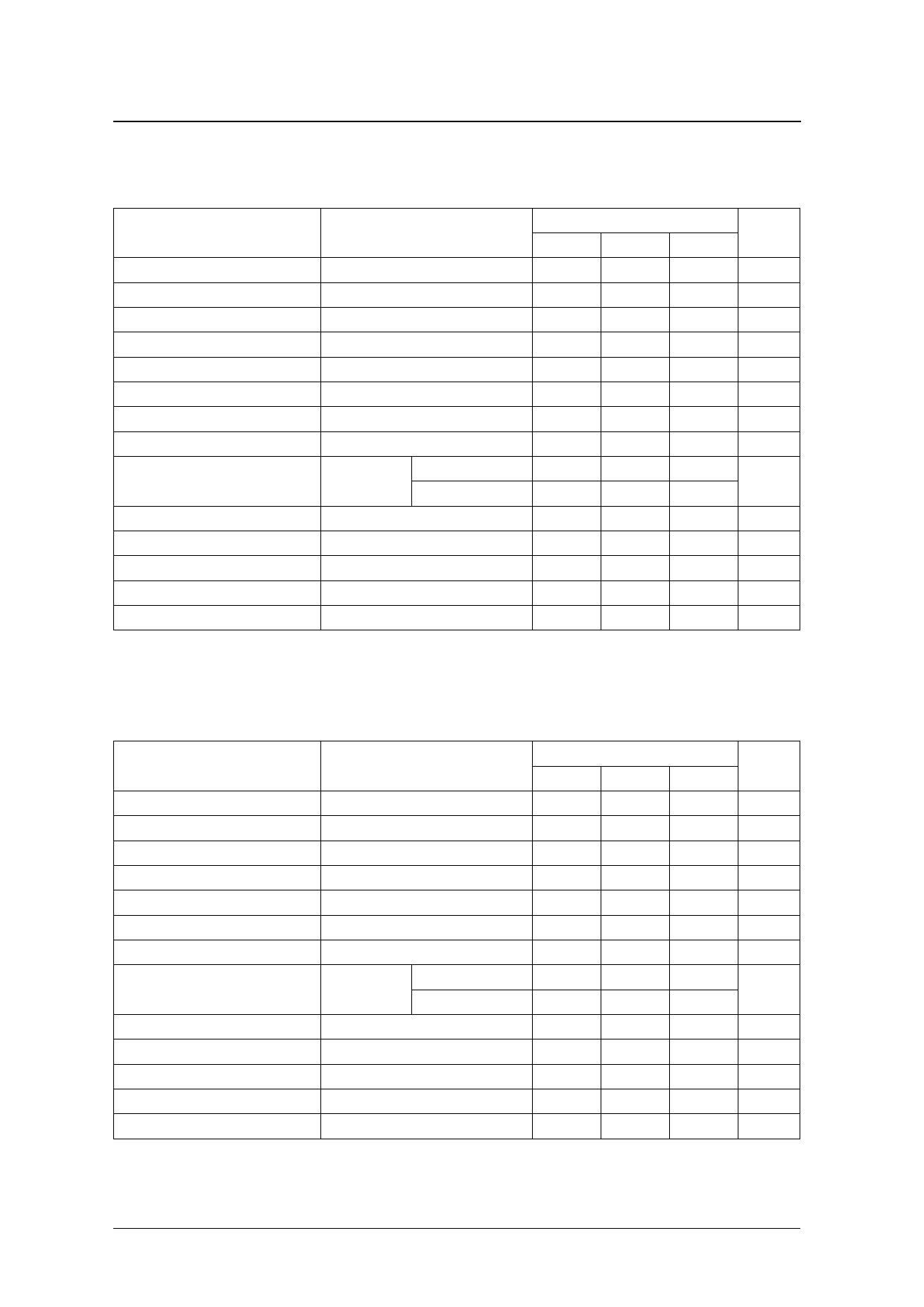
Focus Sample-and-Hold, Low-pass Filter Characteristics (FSUB → FER)
VCC = 5V ± 5%, GND = 0V, Ta = 0 to 70°C, FSUB and FER signals in phase
Parameter
Condition
FSUB input signal range
VREF2 reference
FER output voltage range
VREF2 reference
FER output offset voltage
VREF2 reference, VIN = VREF2
FER output offset voltage temperature drift VREF2 reference
FER output signal slew rate
LPF off
FER output load regulation
FSUB input impedance
IO U T = ±3mA, V IN = V R E F 2
FER output signal gain
FER output signal bandwidth1
FER output gain peaking1
Hold time FER output droop characteristic
S/H acquisition time
FER output hold error
VIN = 1.5Vp-p,
−3dB from DC
LPF off (FFE = HIGH)
LPF on (FFE = LOW)
DC to −3dB frequency
VIN = 200mVp-p, CFHOLD = 1000pF
∆V IN = 200mV, target value ± 10%
With respect to the previous value
Power-down state FER output impedance
1. C L = 20pF, RL = 500Ω
min
−1 . 2 5
−1 . 2 5
–
–
1
–
100
−0 . 1 7
500
115
−3
–
–
–
1
Rating
typ
0
0
–
–
–
–
–
0
–
160
–
–
–
–
–
max
+1.25
+1.25
±8.0
±45
–
±10
–
+0.17
–
230
+0.5
0.025
1
±4
–
Tracking Sample-and-Hold, Low-pass Filter Characteristics (TSUB → TRE)
VCC = 5V ± 5%, GND = 0V, Ta = 0 to 70°C, TSUB and TRE signals in phase
Parameter
Condition
TSUB input signal range
VREF2 reference
TRE output voltage range
VREF2 reference
TRE output offset voltage
VREF2 reference, VIN = VREF2
TRE output offset voltage temperature drift VREF2 reference
TRE output load regulation
TSUB input impedance
IO U T = ±3mA, V IN = V R E F 2
TRE output signal gain
TRE output signal bandwidth1
TRE output gain peaking1
VIN = 1.5Vp-p,
−3dB from DC
TFE = HIGH
TFE = LOW
DC to −3dB frequency
Hold time TRE output droop characteristic
S/H acquisition time
TRE output hold error
VIN = 200mVp-p, CTHOLD = 1000pF
∆V IN = 200mV, target value ±10%
With respect to the previous value
Power-down state TRE output impedance
1. C L = 20pF, RL = 500Ω
min
−1 . 2 5
−1 . 2 5
–
–
–
100
−0 . 1 7
24
115
−3
–
–
–
1
Rating
typ
0
0
–
–
–
–
0
35
160
–
–
–
–
–
max
+1.25
+1.25
±8.0
±45
±10
–
+0.17
50
230
+0.5
0.025
1
±4
–
Unit
V
V
mV
µ V / °C
V/µs
mV
kΩ
dB
kHz
dB
%/µs
µs
mV
MΩ
Unit
V
V
mV
µ V / °C
mV
kΩ
dB
kHz
dB
%/µs
µs
mV
MΩ
NIPPON PRECISION CIRCUITS—6
Share Link: 