SL3522 Ver la hoja de datos (PDF) - Zarlink Semiconductor Inc
Número de pieza
componentes Descripción
Fabricante
SL3522 Datasheet PDF : 21 Pages
| |||
SL3522
500MHz 75dB Logarithmic/Limiting Amplifier
Advance Information
Supersedes edition in Professional Products IC Handbook May 1991
DS3534 - 2.0 April 1994
The SL3522 is a monolithic seven stage successive
detection logarithmic amplifier integrated circuit for use in the
100MHz to 500MHz frequency range. It features an on–chip
video amplifier with provision for external adjustment of log
Slope and offset. It also features a balanced RF output. The
SL3522 operates from supplies of ±5V.
FEATURES
s 75dB Dynamic Range
s Surface Mount SO Package
s Adjustable Log Slope and Offset
s 0dBm RF Limiting Output
s 60dBm Limiting Range
s 2V Video Output Range
s Low Power (Typ. 1W)
s
Temperature
Range
(T ):
CASE
-55°C
to
+125°C
APPLICATIONS
s Ultra Wideband Log Receivers
s Channelised and Monpulse Radar
s Instrumentation
ABSOLUTE MAXIMUM RATINGS
Supply Voltage
Storage temperature
Junction temperature
Thermal resistance
Die-to-case
Die-to-ambient
Applied DC voltage to RF input
Applied RF power to RF input
±6.0V
-65°C to +175°C
+175°C
15.5°C/W
76.5°C/W
±400mV
+15dBm
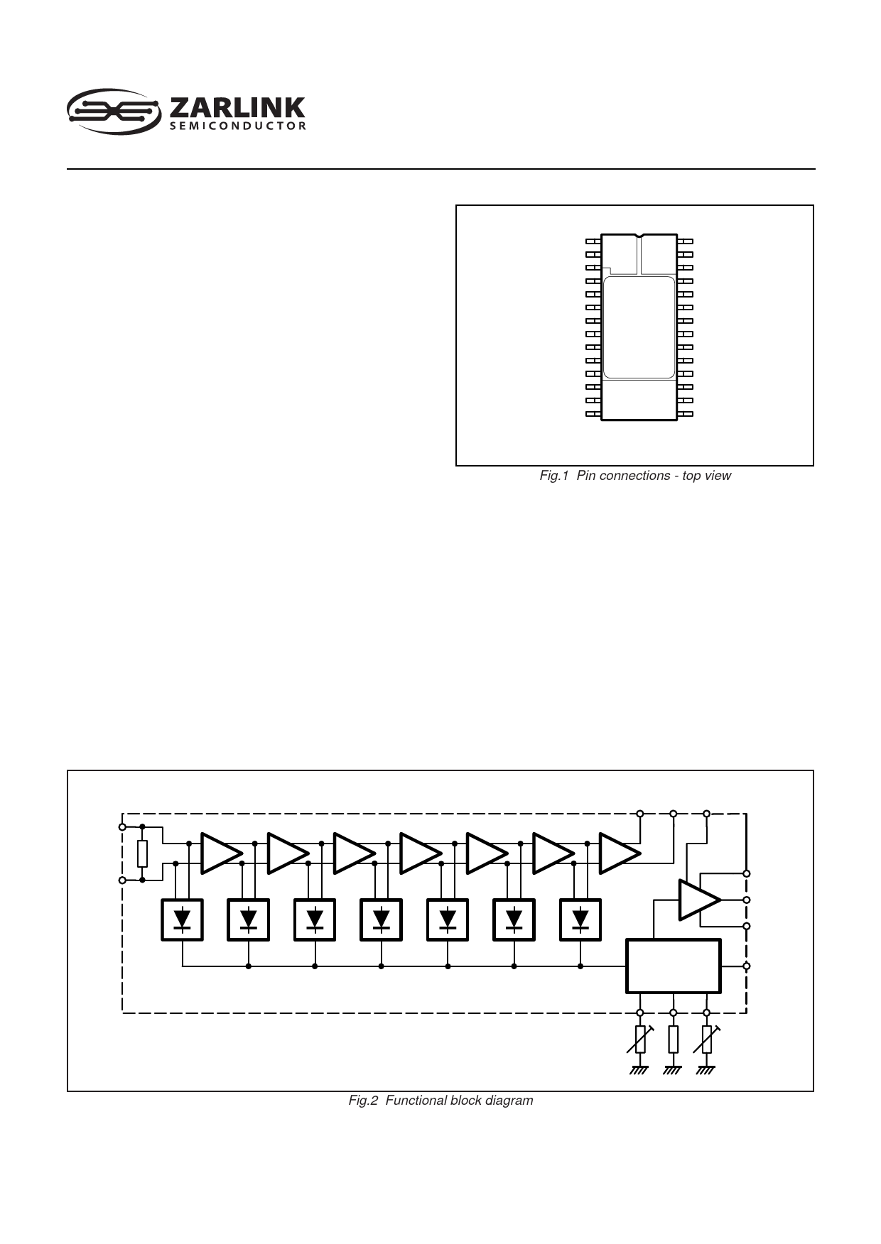
N/C
1
N/C
2
VEE
3
GND
4
VEE
5
GND
6
VEE
7
RF O/P GND
8
RF O/P–
9
RF O/P+
10
RF O/P VEE
11
VIDEO O/P VEE
12
VIDEO O/P
13
VIDEO O/P VCC
14
28
RF I/P+
27
RF I/P–
26
VEE
25
GND
24
VEE
23
GND
22
VEE
21
GND
20
VIDEO VEE
19
GAIN ADJUST
18
TRIM REF
17
OFFSET ADJ
16
VIDEO GND
15
VIDEO VCC
Fig.1 Pin connections - top view
MC28
ORDERING INFORMATION
SL3522 A MC (Miniature Ceramic package)
SL3522 C MC (Miniature Ceramic package)
SL3522 NA 1C (Probe-tested bare die)
(Also available: SL3522 AA MC screened to Zarlink HI-REL
level A. Contact Zarlink Semiconductor sales outlet for a
separate datasheet.)
ESD PROTECTION
To achieve the high frequency performance there are no
ESD protection structures on the RF input pins (27, 28). These
pins are highly static sensitive, typically measured as 250V
using MIL-STD-883 method 3015. Therefore, ESD handling
precautions are essential to avoid degradation of
performance or permanent damage to this device.
RF 27
I/P –
RF
I/P + 28
3, 5, 7, 20, 22, 24, 26 VEE
4, 6, 8, 21, 23, 25 GND
RF RF O/P
O/P– O/P+ VCC
9 10 14
VIDEO GAIN
AND OFFSET
ADJUST
O/P
GND
16
VIDEO
13 OUT
O/P
12 VEE
VIDEO
15 VCC
19 18 17
GAIN
ADJ
OFFSET
RG RT RO ADJ
Fig.2 Functional block diagram
Share Link: 