SL34119 Ver la hoja de datos (PDF) - System Logic Semiconductor
Número de pieza
componentes Descripción
Fabricante
SL34119 Datasheet PDF : 6 Pages
| |||
SL34119
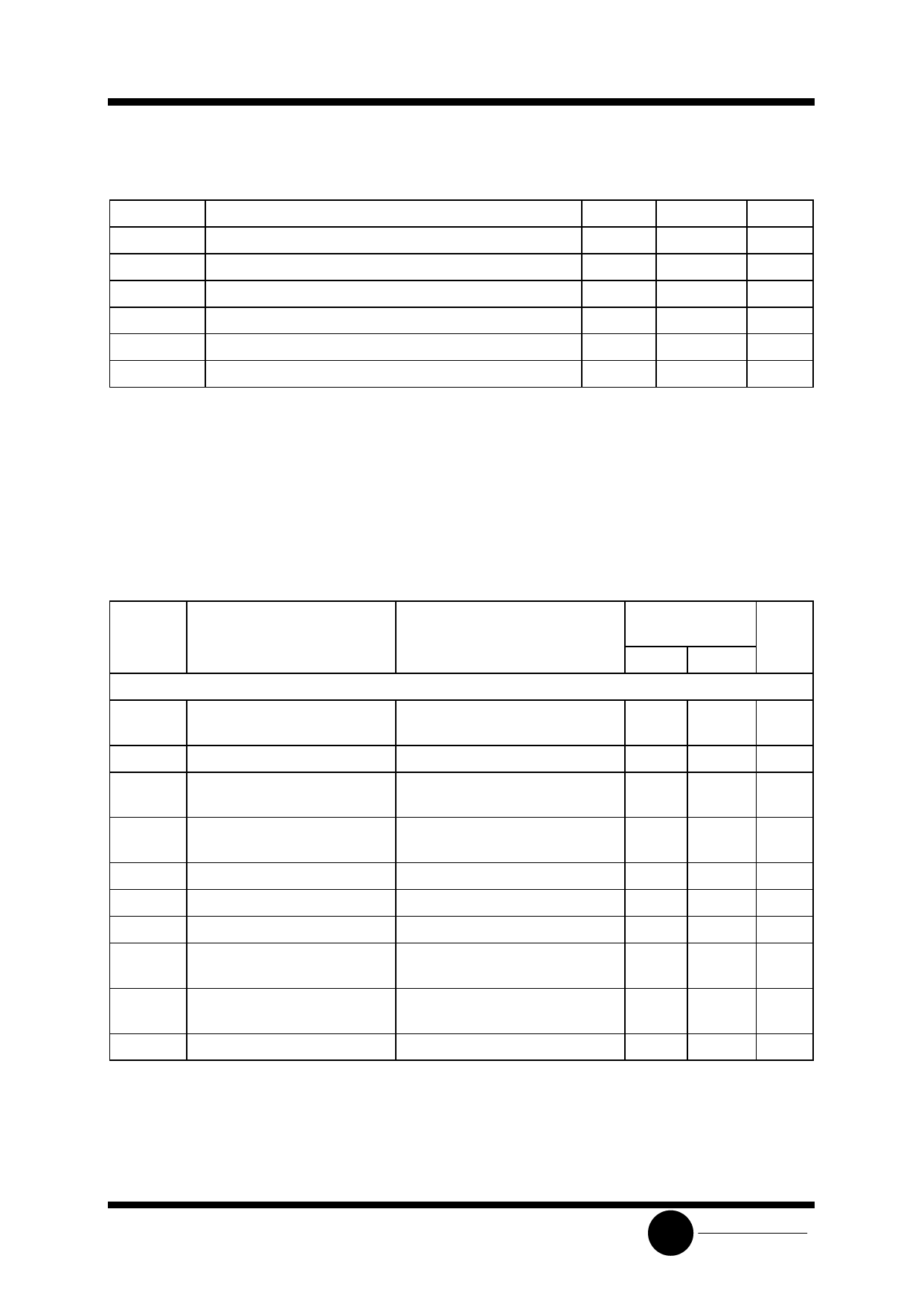
RECOMMENDED OPERATING CONDITIONS
Symbol
Parameter
Min
Max
Unit
VCC
RL
IL
AVD
Supply Voltage
Load Impedance
Peak Load Current
Differential Gain (5.0 KHz bandwidth)
2.0
16
V
8.0
100
Ω
-
200
mA
0
46
dB
VCD
Voltage @ CD (Pin 1)
0
VCC
V
TA
Operating Temperature, All Pakage Types
-10
+70
°C
This device contains protection circuitry to guard against damage due to high static voltages or electric
fields. However, precautions must be taken to avoid applications of any voltage higher than maximum rated
voltages to this high-impedance circuit. For proper operation, VIN and VOUT should be constrained to the range
GND≤(VIN or VOUT)≤VCC.
Unused inputs must always be tied to an appropriate logic voltage level (e.g., either GND or VCC).
Unused outputs must be left open.
ELECTRICAL CHARACTERISTICS(TA = -10 to +70°C, VCD = 0 V)
Symbol
Parameter
Test Conditions
AMPLIFIERS (DC CHARACTERISTICS)
VO
Output DC Level (VO1, VO2)
VOH Output High Level
VOL Output Low Level
∆VO Output DC Offset Voltage
(VO1-VO2)
IIB
Input Bias Current @ VIN
RFC1 Equivalent Resistance @ FC1
RFC2 Equivalent Resistance @ FC2
VIH
Minimum High-Level Input
Voltage
VIL
Maximum Low-Level Input
Voltage
RCD Input Resistance
VCC =3.0 V, RL =16Ω
Rf = 75 KΩ
IOUT = -75 mA, VCC = 2.0 V
IOUT = 75 mA,
2.0 V ≤ VCC ≤ 16 V
VCC =6.0 V, RL =32Ω
Rf = 75 kΩ
VCC =6.0 V
VCC = 6.0 V
VCC = 6.0 V
VCC = VCD = 16 V
Guaranteed
Limits
Unit
Min Max
0.75
1.75
V
0.5
-
V
-
0.55
V
-200
200
mV
-
1600
nA
100
220
KΩ
18
40
KΩ
2.0
-
V
-
0.8
V
50*
175* KΩ
(continued)
SLS
System Logic
Semiconductor
Share Link: 